How to make flexible pcb
Understanding The Basics Of Flexible PCB Design
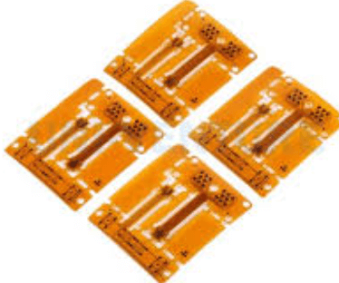
Flexible printed circuit boards (PCBs) have become an integral component in modern electronics, offering a versatile and lightweight alternative to traditional rigid PCBs.
Understanding the basics of flexible PCB design is essential for engineers and designers who wish to leverage their unique advantages.
To begin with, flexible PCBs are constructed using a flexible substrate, typically made from polyimide or polyester materials. These substrates provide the necessary flexibility, allowing the circuit to bend and conform to various shapes and spaces, which is particularly beneficial in compact and dynamic applications.
The design process for flexible PCBs starts with a clear understanding of the application’s requirements.
This involves determining the electrical, mechanical, and environmental constraints that the PCB must withstand. For instance, in applications where the PCB will be subjected to repeated bending, it is crucial to consider the bend radius and the number of flex cycles the board can endure without failure. This ensures the longevity and reliability of the circuit in its intended application.
Once the requirements are established, the next step is to select appropriate materials.
The choice of substrate, copper thickness, and adhesive type plays a significant role in the performance of the flexible PCB. Polyimide is often preferred for its excellent thermal stability and mechanical properties, while polyester may be chosen for cost-sensitive applications. The copper layer, which forms the conductive traces, must be carefully specified to balance flexibility with electrical performance. Thinner copper layers enhance flexibility but may require careful design to handle the required current loads.
Designing the circuit layout is another critical aspect of flexible PCB design.
Unlike rigid PCBs, where traces can be routed in straight lines, flexible PCBs often require curved traces to accommodate bending and flexing. This necessitates the use of specialized design software capable of handling the unique requirements of flexible circuits. Additionally, designers must pay attention to the placement of components and vias, ensuring they do not interfere with the board’s flexibility. Components should be placed in areas that experience minimal bending, and vias should be avoided in regions that will flex frequently.
Thermal management is another important consideration in flexible PCB design.
The materials used in flexible PCBs have different thermal properties compared to rigid boards, which can affect heat dissipation. Designers must account for this by incorporating thermal reliefs and ensuring adequate spacing between heat-generating components. This helps prevent overheating and ensures the reliable operation of the circuit.
Furthermore, the manufacturing process for flexible PCBs differs from that of rigid boards.
It involves additional steps such as coverlay application, which protects the circuit from environmental factors and mechanical stress. Understanding these manufacturing nuances is crucial for designing a board that can be produced efficiently and cost-effectively.
In conclusion, designing flexible PCBs requires a comprehensive understanding of the materials, design principles, and manufacturing processes involved. By carefully considering the application’s requirements, selecting appropriate materials, and employing specialized design techniques, engineers can create flexible PCBs that meet the demands of modern electronic devices. As technology continues to advance, the role of flexible PCBs is likely to expand, making it increasingly important for designers to master the fundamentals of this versatile technology.
Essential Materials And Tools For Flexible PCB Fabrication
In the realm of modern electronics, flexible printed circuit boards (PCBs) have emerged as a pivotal innovation, offering versatility and adaptability in various applications. To embark on the journey of fabricating a flexible PCB, it is crucial to understand the essential materials and tools required for the process. This knowledge not only ensures the successful creation of a functional PCB but also enhances the efficiency and quality of the final product.
To begin with, the primary material for flexible PCB fabrication is the substrate, typically made from polyimide or polyester films.
These materials are chosen for their excellent flexibility, thermal stability, and electrical insulation properties. Polyimide, in particular, is favored for its ability to withstand high temperatures, making it suitable for applications that demand durability under extreme conditions. Alongside the substrate, conductive materials such as copper foil are indispensable. Copper is preferred due to its superior electrical conductivity, which is essential for the efficient transmission of signals across the circuit.
In addition to the substrate and conductive materials, adhesives play a critical role in flexible PCB fabrication.
These adhesives are used to bond the copper foil to the substrate, ensuring a stable and reliable connection. The choice of adhesive is crucial, as it must maintain its integrity under various environmental conditions, including temperature fluctuations and mechanical stress. Commonly used adhesives include acrylic and epoxy-based formulations, each offering distinct advantages depending on the specific requirements of the application.
Transitioning to the tools necessary for flexible PCB fabrication, precision and accuracy are paramount.
A laser cutting machine is often employed to achieve the intricate patterns required for the circuit design. This tool allows for precise cutting of the substrate and copper foil, ensuring that the dimensions and shapes align perfectly with the design specifications. Furthermore, a laminating press is essential for bonding the layers of the PCB together. This tool applies heat and pressure to ensure a uniform and secure adhesion between the substrate and the conductive layers.
Moreover, a drilling machine is indispensable for creating vias and holes in the PCB.
These features are crucial for establishing connections between different layers of the circuit. The drilling process requires meticulous attention to detail, as any deviation can compromise the functionality of the PCB. Additionally, an etching machine is used to remove excess copper from the board, leaving only the desired circuit pattern. This step is vital for defining the electrical pathways and ensuring the proper functioning of the PCB.
Finally, testing and inspection tools are essential to verify the integrity and performance of the fabricated PCB.
Multimeters and oscilloscopes are commonly used to measure electrical parameters and ensure that the circuit operates as intended. Visual inspection tools, such as microscopes, are also employed to detect any physical defects or irregularities in the PCB.
In conclusion, the fabrication of flexible PCBs necessitates a comprehensive understanding of the materials and tools involved in the process. By selecting the appropriate substrate, conductive materials, and adhesives, and utilizing precision tools for cutting, laminating, drilling, and etching, one can achieve a high-quality flexible PCB. This meticulous approach not only ensures the functionality and reliability of the PCB but also paves the way for innovative applications in the ever-evolving field of electronics.
Step-By-Step Guide To Designing A Flexible PCB Layout
Designing a flexible PCB layout requires a meticulous approach, as it involves several unique considerations compared to traditional rigid PCBs. The process begins with understanding the specific requirements of your project, which will guide the design and material selection.
Initially, it is crucial to define the electrical and mechanical constraints,
such as the number of layers, the type of materials, and the flexibility needed for the application. This foundational step ensures that the design will meet the necessary performance standards while maintaining durability.
Once the requirements are clear, the next step involves selecting the appropriate materials.
Flexible PCBs typically use polyimide as the substrate due to its excellent thermal stability and flexibility. Copper is commonly used for the conductive layers, and it is essential to choose the right thickness to balance flexibility and electrical performance. Additionally, the adhesive used to bond the layers must be carefully selected to withstand the environmental conditions the PCB will face.
With materials in hand, the design process can commence using PCB design software.
This software allows for the creation of a schematic that outlines the electrical connections and components. It is important to pay attention to the bend areas, ensuring that traces are routed perpendicular to the bend to minimize stress. Moreover, maintaining a uniform trace width and spacing is vital to prevent potential failures due to mechanical stress.
Transitioning from schematic to layout, the placement of components is a critical step.
Components should be strategically placed to minimize the length of traces, which reduces resistance and potential signal loss. Furthermore, it is advisable to place components that generate heat away from flexible areas to prevent damage. The use of teardrop pads at the junctions of traces and pads can also enhance mechanical strength, reducing the risk of trace lifting.
As the layout progresses, incorporating design rules specific to flexible PCBs is essential.
These rules include maintaining a minimum bend radius, which is typically ten times the thickness of the board, to prevent cracking. Additionally, it is beneficial to use curved traces instead of sharp angles, as this reduces stress concentration. Implementing these design rules ensures the reliability and longevity of the flexible PCB.
After finalizing the layout, a thorough design review is necessary.
This review should check for potential issues such as overlapping traces, insufficient clearances, and violations of design rules. Utilizing design rule check (DRC) features in the software can automate this process, highlighting areas that require attention. Once the design passes the review, it is ready for prototyping.
Prototyping involves fabricating a small batch of the designed PCBs to test their performance in real-world conditions.
This step is crucial for identifying any unforeseen issues that may arise during manufacturing or operation. Testing should include mechanical stress tests, thermal cycling, and electrical performance evaluations. Feedback from this testing phase can inform necessary adjustments to the design before full-scale production.
In conclusion, designing a flexible PCB layout is a complex process that demands careful consideration of materials, design rules, and testing. By following a structured approach and leveraging advanced design tools, engineers can create flexible PCBs that meet the specific needs of their applications, ensuring both functionality and reliability.
Common Challenges And Solutions In Flexible PCB Manufacturing
In the realm of electronics, flexible printed circuit boards (PCBs) have emerged as a pivotal innovation, offering a myriad of advantages over their rigid counterparts. However, the manufacturing of flexible PCBs is not without its challenges. Understanding these challenges and their corresponding solutions is crucial for ensuring the reliability and efficiency of the final product.
One of the primary challenges in flexible PCB manufacturing is material selection.
Unlike rigid PCBs, which predominantly use FR-4 material, flexible PCBs require substrates that can withstand bending and flexing. Polyimide is a popular choice due to its excellent thermal stability and flexibility. However, it is also more expensive and can be difficult to handle. To address this, manufacturers often employ a combination of materials to balance cost and performance, ensuring that the substrate can endure the mechanical stresses it will encounter in its application.
Another significant challenge is the design complexity associated with flexible PCBs.
The need to accommodate bending and twisting necessitates a more intricate design process. Engineers must carefully consider the placement of components and the routing of traces to prevent stress concentration, which can lead to circuit failure. Advanced design software can aid in this process by simulating the mechanical behavior of the PCB under various conditions, allowing designers to optimize the layout before production begins.
The manufacturing process itself presents further challenges, particularly in terms of maintaining dimensional stability.
Flexible PCBs are prone to warping and distortion during fabrication, which can lead to misalignment and defects. To mitigate this, manufacturers often use specialized equipment and techniques, such as vacuum lamination and precision alignment systems, to ensure that the layers of the PCB are accurately aligned and bonded. Additionally, maintaining a controlled environment with stable temperature and humidity levels is essential to prevent material expansion or contraction.
Soldering components onto flexible PCBs also poses unique difficulties.
The heat required for soldering can cause the flexible substrate to deform, potentially damaging the board or the components. To overcome this, manufacturers may use low-temperature soldering techniques or employ heat sinks to dissipate excess heat during the soldering process. Furthermore, the use of surface-mount technology (SMT) can help reduce the thermal stress on the board by minimizing the amount of heat applied.
Testing and quality assurance are critical steps in the flexible PCB manufacturing process, as they help identify defects that could compromise the board’s performance.
However, testing flexible PCBs can be more challenging than testing rigid ones due to their pliability. Automated optical inspection (AOI) systems and X-ray inspection are commonly used to detect defects such as misaligned components or broken traces. Additionally, functional testing under simulated operating conditions can help ensure that the PCB will perform reliably in its intended application.
In conclusion, while the manufacturing of flexible PCBs presents several challenges, these can be effectively managed through careful material selection, advanced design techniques, precise manufacturing processes, and rigorous testing. By addressing these challenges, manufacturers can produce flexible PCBs that meet the demanding requirements of modern electronic devices, paving the way for continued innovation in the field. As technology advances, ongoing research and development will likely yield new solutions and improvements, further enhancing the capabilities and applications of flexible PCBs.


