How to Output PCB Production Files: A Comprehensive Guide
Introduction to PCB Production Files
Printed Circuit Board (PCB) manufacturing requires precise documentation to ensure accurate fabrication of your design. The process of outputting PCB production files is a critical step that bridges your design work with physical board production. These files contain all the necessary information that PCB manufacturers need to transform your electronic design into a functional circuit board.
PCB production files typically include several standardized file formats that collectively describe every aspect of your board’s design – from copper layers and solder mask to silkscreen and drill patterns. Understanding how to properly generate these files ensures that your manufacturer can produce your boards exactly as intended, minimizing errors, delays, and additional costs.
Essential PCB Production Files
Before diving into the output process, it’s important to understand the key files required for PCB production:
- Gerber Files: The industry-standard format that describes each layer of your PCB
- NC Drill Files: Contain information about hole sizes and locations
- Bill of Materials (BOM): Lists all components required for assembly
- Pick and Place Files: Provide component locations and orientations
- Assembly Drawings: Visual guides for PCB assembly
- Fabrication Drawings: Overall board specifications and requirements
- Netlist Files: Electrical connectivity information
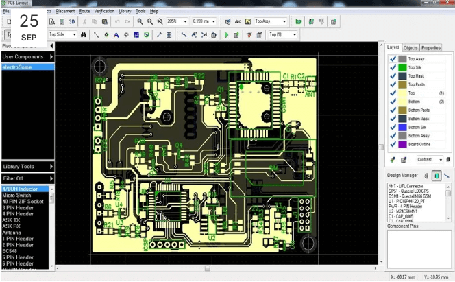
Most PCB design software packages can generate these files, though the specific process may vary between different tools like Altium Designer, Eagle, KiCad, OrCAD, or PADS.
Step-by-Step Guide to Outputting PCB Production Files
1. Final Design Verification
Before generating production files, thoroughly verify your PCB design:
- Run Design Rule Checks (DRC) to identify any violations
- Verify component footprints and pad sizes
- Check layer stackup and material specifications
- Confirm board dimensions and outline
- Review clearance and spacing requirements
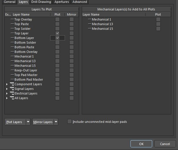
2. Generating Gerber Files
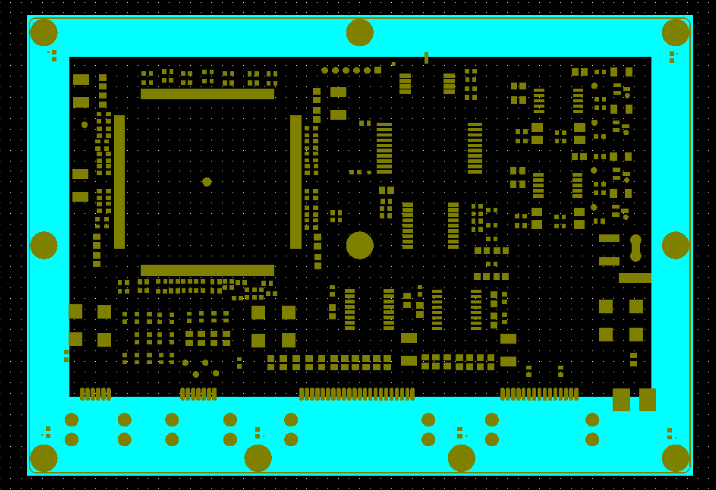
Gerber files (RS-274X format is current standard) represent each layer of your PCB:
- Open your PCB design software and locate the Gerber file generation option
- Select all required layers (typically):
- Top and bottom copper layers
- Solder mask layers (top and bottom)
- Silkscreen layers (top and bottom)
- Board outline/mechanical layer
- Paste mask layers (for SMD components)
- Set appropriate parameters:
- Format: 2:5 (decimal format with 2 integer and 5 decimal places)
- Units: Inches or millimeters (consistent with your design)
- Include aperture files (RS-274X embeds aperture information)
- Generate files with descriptive names (e.g., “TopLayer.GTL”, “BottomMask.GBS”)
3. Creating NC Drill Files
NC (Numerical Control) drill files specify hole locations and sizes:
- Locate the drill file generation option in your software
- Select appropriate settings:
- Format should match your Gerber files (2:5)
- Units consistent with Gerber files
- Generate separate files for plated and non-plated holes if required
- Common formats:
- Excellon format is most widely accepted
- Include tool size information
4. Generating Additional Documentation
Bill of Materials (BOM):
- Export from your schematic or PCB tool
- Include: Reference designators, component values, packages, manufacturers part numbers
- Save as CSV or Excel for easy editing
Pick and Place Files:
- Machine-readable file for automated assembly
- Include: X/Y coordinates, rotation, side of board, reference designator
- Typically CSV or text format
Assembly Drawings:
- PDF or additional Gerber file showing component outlines and locations
- Include reference designators visible
Fabrication Drawings:
- Board outline with critical dimensions
- Layer stackup information
- Special manufacturing notes
5. File Organization and Naming Conventions
Establish a clear naming convention for your production files:
- Use consistent prefixes/suffixes (e.g., .GTL for top layer, .GBL for bottom layer)
- Include revision numbers in filenames
- Create a README file explaining any special requirements
- Organize files in a logical folder structure
Common Gerber file extensions:
- .GTL – Top layer
- .GBL – Bottom layer
- .GTO – Top overlay (silkscreen)
- .GBO – Bottom overlay
- .GTS – Top solder mask
- .GBS – Bottom solder mask
- .GTP – Top paste mask
- .GBP – Bottom paste mask
- .GML or .GM1 – Mechanical/board outline
- .TXT or .DRL – Drill file

Best Practices for PCB File Output
- Always Run DRC Before Exporting: Ensure your design passes all design rule checks before generating production files.
- Use Standardized Naming Conventions: This helps manufacturers quickly understand your file set.
- Include a Layer Stackup Diagram: Especially important for multilayer boards, showing material types and thicknesses.
- Provide Complete Documentation: Don’t assume manufacturers will know your intentions – include notes on special requirements.
- Verify Files Before Submission:
- Use Gerber viewers to check all layers
- Confirm drill files align with your design
- Check that all critical dimensions are correct
- Communicate Special Requirements Clearly:
- Impedance control needs
- Special surface finishes
- Any non-standard materials
- Testing requirements
- Archive Complete Sets: Keep full sets of production files for each revision to maintain proper version control.
Common Pitfalls to Avoid
- Incorrect Units or Formats: Mixing inches and millimeters or using wrong decimal places can cause manufacturing errors.
- Missing Layers: Forgetting to include critical layers like solder mask or silkscreen.
- Inadequate Clearances: Not accounting for manufacturing tolerances in your design.
- Outdated Specifications: Using obsolete file formats or standards.
- Incomplete Documentation: Failing to provide all necessary supporting files and information.
- Assuming Manufacturer Defaults: Not specifying requirements because you assume the manufacturer will use certain defaults.
Advanced Considerations
For HDI (High Density Interconnect) Boards:
- Additional files may be needed for microvias and complex layer transitions
- More detailed stackup information required
- Tighter tolerances must be clearly specified
For Flex/Rigid-Flex Boards:
- Include bend area diagrams and radius specifications
- Provide material specifications for flexible layers
- Include stiffener locations and materials
For High-Speed Designs:
- Impedance control requirements must be detailed
- Include signal integrity analysis if available
- Specify material dielectric properties if critical
Verifying Your Output Files
Before sending files to your manufacturer:
- Use Gerber Viewers: Tools like GC-Prevue, GerbView, or online viewers allow you to inspect each layer.
- Check Layer Alignment: Ensure all layers align properly when viewed together.
- Verify Drill Files: Confirm hole sizes and locations match your design intent.
- Review Documentation: Double-check that all supporting documents are complete and accurate.
- Consider DFM Analysis: Some software can perform Design for Manufacturability checks on your output files.
Submitting Files to Your Manufacturer
When ready to submit:
- Package All Files: Create a zip file containing the complete set of production files.
- Include Instructions: Provide any special notes or requirements in a README file.
- Choose Submission Method:
- Manufacturer’s web portal
- Email (for smaller files)
- FTP or cloud storage for larger files
- Follow Up: Confirm receipt of files and expected timeline for manufacturing.
Conclusion
Properly outputting PCB production files is a critical skill for any electronics designer. By following standardized procedures, using consistent naming conventions, and thoroughly verifying your files before submission, you can significantly reduce manufacturing errors and delays. Remember that clear communication with your manufacturer through complete documentation is just as important as the technical aspects of file generation.
As PCB technology continues to advance with higher densities and more complex requirements, the importance of accurate production file generation only increases. Investing time to master this process will pay dividends in smoother manufacturing experiences and higher quality end products.
Always keep in mind that your production files are the sole communication channel between your design intent and the physical realization of your PCB. Taking the extra time to ensure these files are complete, accurate, and clearly documented will help turn your design into a successfully manufactured circuit board.