How to overcome the most common manufacturing errors when making PCBs
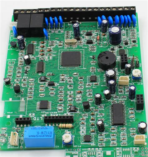
When it comes to PCB manufacturing, we may see quite a bit of complexity due to the widespread use of multi-layer boards with up to 36 layers. However, the result it brings is the possibility of errors, which can be very costly. Therefore, there is a pressing need to focus on common PCB manufacturing errors so that they can be avoided. Here is a complete list of errors to watch out for:
1.Flex Cracks
Cause:
In short, this error occurs when the PCB is bent excessively due to ceramic chip capacitors.
Solution:
The simple way to solve this problem is to change the size of the capacitor. Using small capacitors can successfully solve this problem.
2. Clearance Constraints
Cause:
This is a fairly common PCB manufacturing error. This occurs when clearance constraints are not taken into account when designing the board.
Solution:
To ensure that this problem does not occur, the manufacturing capabilities need to be understood before production so that the board can be designed accordingly.
3. Insufficient Power
Cause:
If the power supply is insufficient during the build phase, it may affect the functionality of the board.
Solution:
Visual inspection and cold testing can ensure that the board power is checked and there are no unexpected underpowering situations.
4. Mechanical Issues
Cause:
If the components are not well fixed to the board or placed too close, a wide range of mechanical issues can occur.
Solution:
It is important to carefully check the dimensions of all components and allow enough space for each component so that any problems can be avoided.
5. Impedance Control
Cause:
Some PCB designs have components that require impedance controlled routing. This requires following the manufacturer’s specifications.
Solution:
To ensure that no problems are encountered, it is important to do the manufacturer’s specifications beforehand and follow them closely.
6. Drill Constraints
Cause:
The drill capability of the manufacturer is an important aspect to know beforehand. Typically, drill sizes range from 6 to 14 mm.
Solution:
7. Through Holes
Cause:
As part of the PCB manufacturing services, it is important to drill holes for through holes. The holes are plated in turn. If the copper layer is not attached to the surface during the electroplating process, it will cause discontinuities. This, in turn, can lead to a host of issues in the PCB.
Solution:
To avoid this problem, it is important to ensure that the holes are drilled smoothly. Rough or fast drilling can lead to flawed holes and also uneven copper deposition. To ensure that this does not happen, it is necessary to use recommended tools and apply appropriate force for drilling. Any lapses in both of these aspects can lead to PCB fab issues.
8. Leaking solder mask
Cause:
This problem occurs when the space between pads is restricted. With closely packed pads, in turn, it affects the deposition of the solder mask. This can also lead to short circuits, making it prone to rust, in addition to affecting the life of the PCB.
Solution:
This problem needs to be sidestepped at the design stage itself. The following issues need to be strictly adhered to:
l Copper pad size
l Clearance
l Copper trace
If these are taken care of, copper mask between pads will not be a problem.