How to prevent PCB warpage
How to prevent PCB warpage
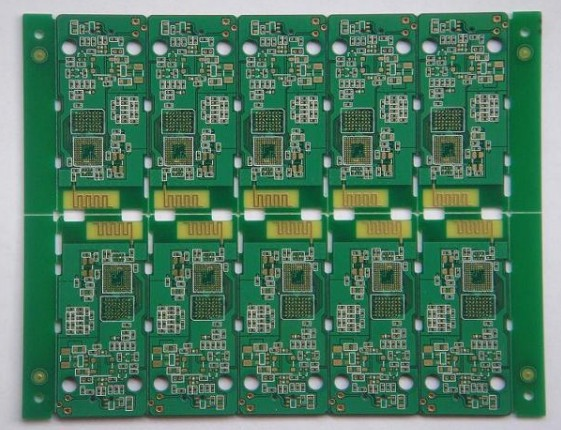
Warping circuit boards can cause misalignment of the components. When the circuit board is bent at SMT or THT, the components and pins are not full, which will bring a lot of difficulties to the assembly and installation work.
IPC-6012, SMB – SMT boards have a maximum warp or twist of 0.75% and other boards generally have warps of less than 1.5%; the allowable warpage (duplex / multilayer) of the electronics assembly plant is typically 0.70 — 0.75%, (1.6mm thickness) In fact, many boards such as SMB, BGA board warpage less than 0.5%; some factories even less than 0.3%; PC-TM-650 2.4.22B
Warpage calculation method = warpage height / length of curved edge
Prevention of board warpage:
1, Engineering design: The arrangement of the prepregs should correspond to each other. The same supplier product should be used for the multi-layer core board and the prepregs. The outer C / S surface area should be as close as possible and an independent grid can be used.
The company is located in:
2, drying board before cutting
The company is located in:
Generally 150 degrees 6 – 10 hours, remove the water vapor inside the board, to further cure the resin completely to eliminate the stress inside the board; preheating bake board, either inside or both sides need!
3, multilayer laminated board should pay attention to the latitude and longitude direction before curing plate:
The company is located in:
Warp and weft to shrink ratio is not the same, the prepreg Laying Layers pay attention to distinguish the latitude and longitude direction; core material should also pay attention to the warp and weft direction; general board curing sheet roll direction is warp; CCL longitude direction;
4, Laminated thickness to eliminate stress plate cold, trim edge;
The company is located in:
5, before drying bake board: 150 degrees 4 hours;
6, the best sheet without mechanical brushing, it is recommended to use chemical cleaning; plating when the use of special fixtures to prevent bending the board folded
The company is located in:
7, after the tin spray on the flat marble or steel cooling to room temperature or air bed cooling and cleaning;
The company is located in:
Warp board processing:
150 degrees or hot 3 – 6 hours, with flat and smooth steel pressure, 2-3 times baking!
Grace Zheng
Email: sales06@andwinpcb.com