How to quickly adjust the silkscreen position number of PCB component?
For later component assembly,especially manual assembly,a PCB assembly drawing is usually drawn for component placement and positioning .At this time,the silkscreen position number shows its necessity.
Friends who are new to PCB drawing must have experienced this operation.Manually adjusting the silkscreen position number of components one by one is very tedious and inefficient…
Is there any good solution?
The silkscreen position number on the PCB can be displayed or hidden during production,but ir does not affect the output of the assembly drawing.Press the shortcut key”L”and press the All Layers Close button to close all layers.Then,select only the silkscreen layer and the corresponding solder mask layer to adjust the silkscreen.The following are the principles and general recommended sizes for adjusting the silkscreen position number:
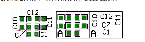
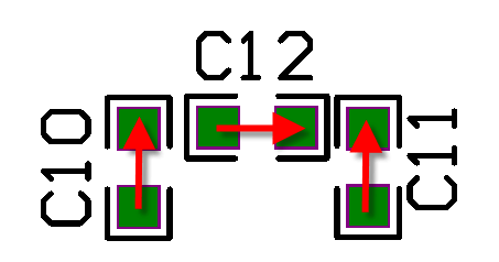
(1)The silkscreen position number is not on the solder mask,and it will be missing after the silkscreen is placed in production.(2)The silk screen position number should be clear.The recommended font width/height size is 4/25mil, 5/30mil, and 6/45mil. (3) Maintain the same direction. Generally, do not place the characters in more than two directions on a PCB. It is recommended that the letters be on the left or at the bottom, as shown in Figure 11-21. bdf6773a-6f77-11ed-8abf-dac502259ad0.png Figure 11-21 Silk screen position number display direction (4) For some silk screen logos that are placed in a left-right direction, you can use 2D auxiliary lines or blocks to mark them for easy reading, as shown in Figure 11-22.
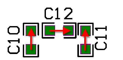
Figure 11-22 Auxiliary lines and blocks
How to adjust the silk screen position number
AltiumDesigner provides a quick way to adjust the silk screen, namely the “Component Text Position” function, which can quickly place the silk screen of a component around or in the center of the component.
(1) Select the component to be operated.
(2) Press the shortcut key “AP” to enter the “Component Text Position” dialog box, as shown in Figure 11-23. This dialog box provides two placement methods: “Identifier” and “Comment”. Here, “Identifier” is used as an example.
(3) “Identifier” provides several directions: up, down, right, left, upper left, lower left, upper right, and lower right, which can correspond to the number keys on the numeric keypad. To quickly place the silkscreen designator of a selected component above it by setting a shortcut key for the “Component Text Position” command, press the numeric keys “5” and “2” on the keypad, as shown in Figure 11-24. The same procedure applies to other placements. For example, pressing the numeric keys “5” and “6” places it to the right of a component, while pressing the numeric keys “5” and “8” places it below it.
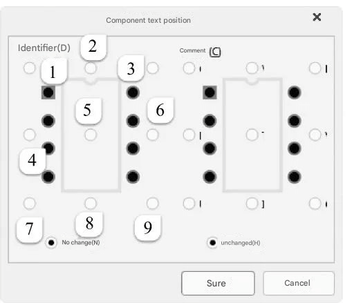
Figure 11-23 “Component Text Position” Dialog Box
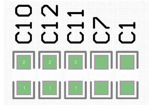
Figure 11-24 Quickly Place the Silkscreen Designator Above the Component
PCB Design Tips
- How to Choose PCB Material?
Selecting PCB material requires a balance between meeting design requirements, manufacturability, and cost. Design requirements encompass both electrical and mechanical aspects. Material considerations are particularly important when designing very high-speed PCBs (frequencies exceeding GHz). For example, the commonly used FR-4 material has a significant dielectric loss at frequencies exceeding several GHz, significantly affecting signal attenuation and making it unsuitable. From an electrical perspective, it’s important to consider whether the dielectric constant and dielectric loss are suitable for the designed frequency.
- How to Avoid High-Frequency Interference?
The basic approach to avoiding high-frequency interference is to minimize the electromagnetic interference of high-frequency signals, also known as crosstalk. This can be achieved by increasing the distance between high-speed and analog signals or by adding ground guards/shunt traces near the analog signals. Also, be mindful of the noise interference from the digital ground to the analog ground.
- How to address signal integrity in high-speed PCB design?
Signal integrity is fundamentally an impedance matching issue. Factors that affect impedance matching include the signal source architecture and output impedance, the characteristic impedance of the trace, the characteristics of the load, and the trace topology. The solution is to use termination and adjust the trace topology.
- Can a ground line be added between differential signal lines?
A ground line is generally not allowed between differential signal lines. The key principle of differential signaling is to leverage the benefits of coupling between differential signals, such as flux cancellation and noise immunity. Adding a ground wire in the middle will destroy this coupling effect.
- When routing a clock, is it necessary to shield the ground wires on both sides?
Whether to add a shielded ground wire depends on the crosstalk/EMI situation on the board. Improper handling of the shielded ground wire can even worsen the situation.
- How do I fix fragmented traces (marked by small boxes) when routing using Allegro?
This occurs because after reusing modules, an automatically named group is automatically generated. The key to resolving this issue is to break up the group. Select the group in the PlacementEdit mode and then break it up.
After completing this command, move all traces within the small boxes by clicking the ix00 coordinates.
- How can I meet EMC requirements as much as possible without incurring excessive cost pressures?
Increased costs on PCBs due to EMC are typically due to increasing the number of ground planes to enhance shielding and adding high-frequency harmonic suppression devices such as ferrite beads and chokes. Furthermore, other shielding structures are often required to ensure the entire system meets EMC requirements. The following are just a few PCB design tips for reducing electromagnetic radiation generated by circuits:
1) Whenever possible, use components with slower signal slew rates to reduce the high-frequency components generated by the signal.
2) Pay attention to the placement of high-frequency components; avoid placing them too close to external connectors.
3) Pay attention to impedance matching of high-speed signals, routing layers, and their return current paths to reduce high-frequency reflections and radiation.
4) Place sufficient and appropriate decoupling capacitors at the power pins of each component to mitigate noise on the power and ground planes. Pay particular attention to whether the capacitors’ frequency response and temperature characteristics meet design requirements.
5) The ground plane near external connectors can be appropriately separated from the ground plane, and the connector ground plane should be connected to the chassis ground as close as possible.
6) Ground guards/shunt traces can be appropriately used near particularly high-speed signals, but be aware of the impact of guards/shunt traces on the characteristic impedance of the traces.
7) The power plane should be set back 20H from the ground plane, where H is the distance between the power plane and the ground plane.
- What rules should be followed for microstrip design in high-frequency PCB designs above 2G?
RF microstrip design requires the use of a 3D field analysis tool to extract transmission line parameters. All rules should be specified within this field extraction tool.
- Which end of a PCB board is best for AC coupling of high-speed signals?
You often see different approaches, some near the receiving end and some near the transmitting end.
Let’s first look at the role of AC coupling capacitors. They generally have three key points: ① The DC voltage at the source and sink ends is different, so they block DC; ② DC crosstalk may be introduced during signal transmission, so blocking DC improves the signal eye diagram; ③ AC coupling capacitors can also provide DC bias and overcurrent protection. Ultimately, the function of an AC coupling capacitor is to provide a DC bias, filter out the DC component of the signal, and make the signal symmetrical about the zero axis.
So why add an AC coupling capacitor? Of course, there are benefits. Adding an AC coupling capacitor definitely improves communication between the two stages and improves noise margins. It’s important to note that AC coupling capacitors typically represent impedance discontinuities in high-speed signals and can cause signal edges to slow.
1) Some protocols or manuals will provide design requirements, and we should follow these placement guidelines.
2) If the first requirement isn’t met, if it’s IC-to-IC, place it close to the receiver.
3) If it’s IC-to-connector, place it close to the connector.
- How can we verify that PCBs meet design process requirements before shipment?
Many PCB manufacturers perform a power-on network continuity test before shipping completed PCBs to ensure that all connections are correct. Furthermore, an increasing number of manufacturers are using X-ray testing to detect defects during etching or lamination. For finished boards after SMT fabrication, ICT testing is generally used, which requires adding ICT test points during PCB design. If a problem occurs, a special X-ray inspection device can be used to rule out whether the fault is caused by processing.


