How to Reduce AC and DC Induced PCB Noise
Introduction
Printed Circuit Board (PCB) noise is one of the most challenging issues in modern electronic design, affecting signal integrity, power quality, and overall system performance. Both alternating current (AC) and direct current (DC) can induce various types of noise in PCBs, leading to electromagnetic interference (EMI), crosstalk, ground bounce, and other undesirable effects. As electronic devices become more complex and operate at higher frequencies, managing PCB noise has become increasingly critical.
This article provides a comprehensive guide on reducing AC and DC induced PCB noise through proper design techniques, layout strategies, component selection, and noise mitigation approaches. By implementing these best practices, engineers can significantly improve the signal quality and reliability of their electronic systems.
Understanding PCB Noise Sources
Before addressing noise reduction techniques, it’s essential to understand the different noise sources in PCBs:
AC-Induced Noise
- Electromagnetic Interference (EMI): Radiated or conducted noise from high-frequency signals
- Crosstalk: Unwanted coupling between adjacent traces
- Ground Loops: Current flow in ground paths creating voltage differences
- Switching Noise: High-frequency transients from digital circuits or power converters
DC-Induced Noise
- Ground Bounce: Voltage fluctuations in ground reference due to high current demands
- Power Supply Ripple: Variations in DC voltage from imperfect regulation
- Thermal Noise: Random electron motion in conductors (Johnson-Nyquist noise)
- DC Bias Effects: Component parameter variations due to DC voltage stress
PCB Layout Strategies for Noise Reduction
1. Proper Grounding Techniques
- Use a Solid Ground Plane: A continuous ground plane provides a low-impedance return path and reduces ground loops
- Implement Star Grounding: Connect all ground returns to a single point for sensitive analog circuits
- Separate Analog and Digital Grounds: Use separate ground planes with a single connection point to prevent digital noise from coupling into analog signals
- Avoid Ground Splits: Unless absolutely necessary, as they can create antenna effects and increase EMI
2. Power Distribution Network Design
- Use Power Planes: Dedicated power planes reduce impedance and provide better decoupling
- Implement Proper Decoupling: Place decoupling capacitors close to IC power pins (0.1μF ceramic capacitors for high frequencies, larger electrolytic for low frequencies)
- Hierarchical Power Distribution: Use multiple voltage domains with appropriate filtering between them
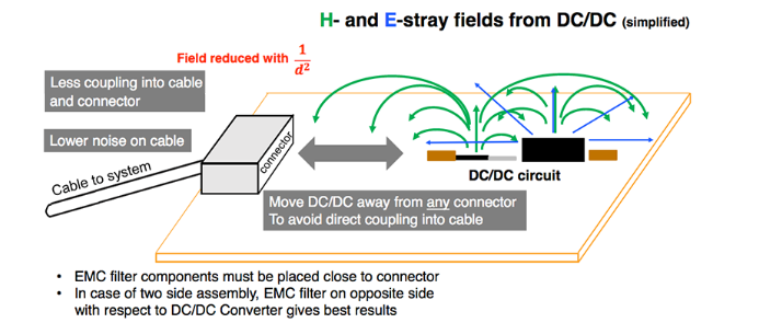
- Minimize Power Loop Areas: Keep power and ground paths close together to reduce inductive effects
3. Trace Routing Best Practices
- Keep High-Speed Signals Short: Minimize trace length for clock signals and other fast edges
- Maintain Proper Trace Spacing: Follow the 3W rule (trace spacing ≥ 3× trace width) to reduce crosstalk
- Avoid Right-Angle Bends: Use 45° angles or curved traces to prevent impedance discontinuities
- Route Sensitive Signals First: Prioritize clock lines, analog signals, and other critical traces
- Use Differential Pairs: For high-speed signals to improve noise immunity
4. Layer Stackup Considerations
- Use Multiple Layers: Four or more layers allow dedicated power and ground planes
- Proper Layer Arrangement: Signal layers should be adjacent to ground planes (e.g., Signal-Ground-Power-Signal)
- Controlled Impedance: Design traces with specific impedance for high-speed signals
- Minimize Via Stubs: Use blind or buried vias for high-frequency designs
Component Selection and Placement
1. Component Selection
- Choose Low-Noise Components: Select ICs with good power supply rejection ratios (PSRR)
- Use Surface-Mount Devices (SMDs): They have lower parasitic inductance than through-hole components
- Select Appropriate Bypass Capacitors: Consider dielectric material (X7R or better for stability), package size, and ESL/ESR
2. Component Placement
- Group Related Components: Keep analog, digital, and power sections physically separated
- Place Decoupling Capacitors Close to ICs: Minimize the loop area between capacitor, IC, and ground
- Orient Components to Minimize Crosstalk: Position sensitive components away from noise sources
- Consider Thermal Management: Heat can increase component noise and affect performance
Filtering and Shielding Techniques
1. Filtering Methods
- RC Filters: For low-frequency noise reduction on signal lines
- LC Filters: For power supply noise suppression
- Ferrite Beads: Effective for high-frequency noise blocking while allowing DC to pass
- Common-Mode Chokes: Reduce common-mode noise in differential signals
2. Shielding Approaches
- Copper Pours: Use grounded copper fills around sensitive traces
- Shield Cans: Metal enclosures for particularly sensitive circuits
- Cable Shielding: Properly terminate shielded cables to prevent antenna effects
- Via Fencing: Rows of grounded vias around high-speed signals to contain EMI
Power Supply Noise Reduction
1. DC Power Noise Mitigation
- Use Linear Regulators: For sensitive analog circuits where switching noise is unacceptable
- Implement Proper Filtering: Multi-stage LC filters for switching power supplies
- Minimize Trace Resistance: Use wide traces or planes for high-current paths
- Remote Sensing: For critical voltage rails to compensate for IR drops
2. AC Power Considerations
- Proper Rectification: Use full-bridge rectifiers with adequate filtering for AC-DC conversion
- Inrush Current Limiting: Prevent large transient currents during power-up
- Isolation Transformers: For sensitive equipment connected to noisy AC mains
- Surge Protection: TVS diodes or MOVs to suppress line transients
Signal Integrity Practices
1. Transmission Line Techniques
- Impedance Matching: Properly terminate transmission lines to prevent reflections
- Controlled Rise Times: Use series resistors to reduce edge rates when possible
- Stub Length Management: Keep stubs short compared to signal wavelength
2. Clock Distribution
- Use Low-Jitter Clock Sources: Important for high-speed digital systems
- Proper Clock Routing: Route clocks as point-to-point connections when possible
- Clock Termination: Match impedance to prevent reflections
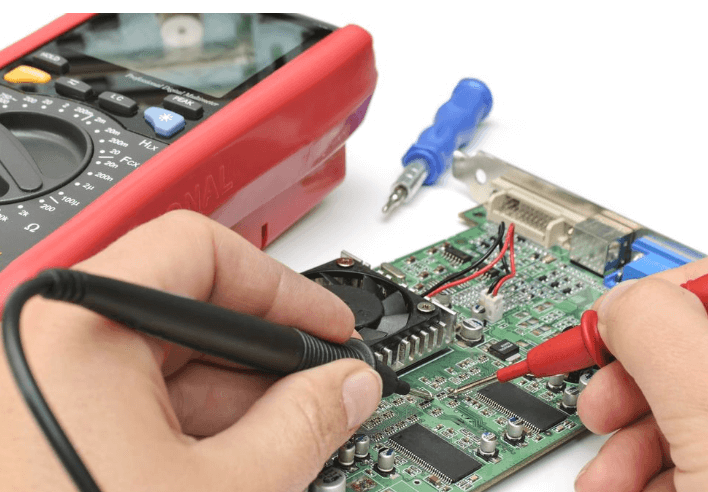
Measurement and Verification
1. Testing Methods
- Power Integrity Analysis: Measure power rail noise with oscilloscopes
- Time Domain Reflectometry (TDR): For impedance verification
- Network Analysis: Evaluate frequency response of critical paths
- Near-Field Scanning: Identify EMI hotspots
2. Troubleshooting Techniques
- Identify Noise Sources: Use spectrum analyzers to characterize noise
- Evaluate Ground Quality: Measure ground bounce with high-bandwidth probes
- Assess Decoupling Effectiveness: Measure impedance versus frequency
Advanced Techniques
1. For High-Speed Designs
- Pre-Emphasis and Equalization: Compensate for channel losses
- Eye Diagram Analysis: Evaluate signal quality in high-speed links
- DDR Routing Guidelines: Follow manufacturer recommendations for memory interfaces
2. For Mixed-Signal Systems
- Careful ADC/DAC Placement: Position near the analog-digital boundary
- Sampling Clock Considerations: Use clean clocks for data converters
- Anti-Aliasing Filters: Properly implement for all ADC inputs
Conclusion
Reducing AC and DC induced PCB noise requires a systematic approach that begins with proper design and continues through careful layout, component selection, and verification. By implementing the techniques discussed in this article—including optimal grounding strategies, power distribution design, careful routing practices, and appropriate filtering—engineers can significantly reduce noise-related issues in their PCB designs.
Remember that noise reduction is often about managing trade-offs between various design constraints. The most effective designs consider noise mitigation from the earliest stages of the design process rather than attempting to fix problems after the board is fabricated. As electronic systems continue to increase in speed and complexity, mastering these noise reduction techniques will become even more critical for successful product development.
By applying these principles and continually staying informed about emerging best practices, designers can create PCBs that meet stringent performance requirements while minimizing noise-related problems throughout the product lifecycle.