How to Repair PCB Vias: A Comprehensive Guide
Introduction to PCB Via Repair
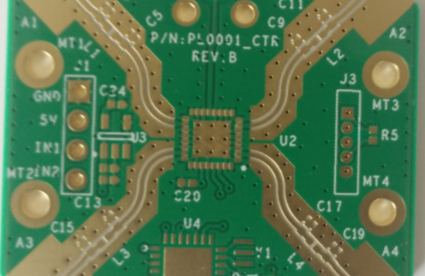
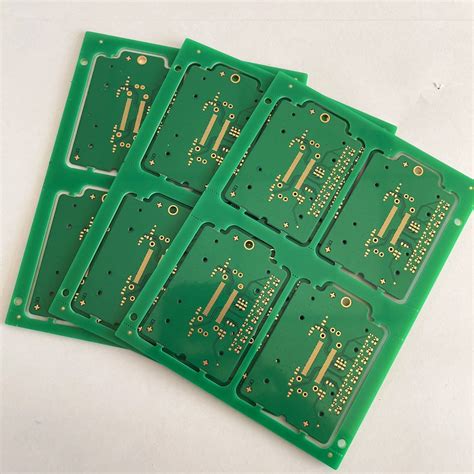
Printed Circuit Board (PCB) vias are essential conductive pathways that connect different layers of a multilayer PCB. These small holes plated with conductive material allow electrical signals and power to travel between layers, making them critical components in modern electronics. When vias become damaged or fail, it can lead to circuit malfunctions, signal integrity issues, or complete device failure.
Via damage can occur during manufacturing, assembly, or throughout the product’s lifecycle due to thermal stress, mechanical shock, or environmental factors. Repairing these vias requires precision, the right tools, and proper techniques to restore electrical connectivity without compromising the board’s integrity.
This comprehensive guide will explore various methods for repairing PCB vias, from simple conductive ink solutions to more advanced micro-repair techniques used by professional repair services.
Understanding Via Types and Common Failure Modes
Types of PCB Vias
- Through-hole vias: Span the entire thickness of the PCB
- Blind vias: Connect an outer layer to one or more inner layers but don’t go through the entire board
- Buried vias: Connect inner layers without reaching outer layers
- Microvias: Small vias (typically <0.15mm) used in high-density designs
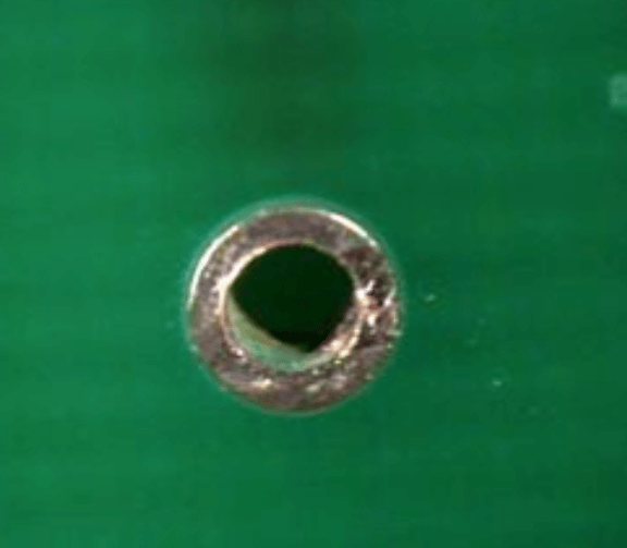
Common Via Failure Modes
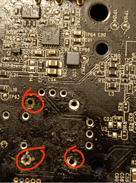
- Plating cracks: Due to thermal cycling or mechanical stress
- Barrel fractures: Complete separation of via plating
- Pad lifting: When the via pad separates from the substrate
- Contamination: Solder mask or debris blocking conductivity
- Corrosion: Environmental factors degrading the conductive material
Tools and Materials Needed for Via Repair
Before attempting any via repair, gather the appropriate tools and materials:
Essential Tools:
- High-quality microscope (10x-40x magnification)
- Precision soldering iron with fine tips (0.2mm-0.5mm)
- Temperature-controlled hot air station
- Conductive epoxy applicator or syringe
- Fiberglass scratch pen or very fine abrasive
- Isopropyl alcohol (99% purity) and cleaning swabs
- Tweezers (non-magnetic, ESD-safe)
- Multimeter for continuity testing
Repair Materials:
- Conductive silver epoxy or ink
- Low-resistance solder paste
- Via plugs or micro-pins
- UV-curable solder mask
- Copper foil or pre-formed via patches
- Flux (no-clean preferred)
Step-by-Step Via Repair Methods
Method 1: Conductive Epoxy Repair (For Simple Via Damage)
- Clean the area: Remove any contamination with isopropyl alcohol
- Prepare the via: Lightly abrade the damaged area with a fiberglass pen
- Apply conductive epoxy: Fill the via carefully using a fine applicator
- Cure the epoxy: Follow manufacturer’s instructions (heat or UV)
- Test continuity: Verify electrical connection between layers
- Apply protective coating: Use conformal coating if needed
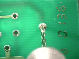
Method 2: Soldering Repair (For Through-hole Vias)
- Clean the via: Remove old solder and oxidation
- Apply flux: To ensure proper solder flow
- Insert a thin wire: Use a small gauge wire as a conductor
- Solder both sides: Ensure complete barrel filling
- Trim excess: Carefully cut any protruding wire
- Test and clean: Verify connection and remove flux residues
Method 3: Micro-pin Insertion (For High-reliability Repairs)
- Enlarge the via slightly: Using a precision drill (if necessary)
- Select appropriate pin: Should fit snugly in the via
- Insert the pin: With conductive adhesive if needed
- Solder both ends: To adjacent traces or pads
- Reinforce structure: With additional epoxy if required
Method 4: Plating Restoration (For Professional Repairs)
- Clean and prepare: Remove all contaminants
- Apply conductive seed layer: Using special solutions
- Electroplate copper: To rebuild the via barrel
- Finish with protective coating: Prevent future corrosion
Advanced Techniques for High-Density PCB Via Repair
Laser-Assisted Via Repair
- Uses focused laser to clean and prepare vias
- Enables precise material deposition
- Particularly useful for microvias
Focused Ion Beam (FIB) Deposition
- Nanoscale repair capability
- Deposits conductive material exactly where needed
- Requires specialized equipment
Conductive Atomic Force Microscopy (CAFM)
- For nanoscale via characterization
- Helps identify exact failure points
- Enables ultra-precise repairs
Best Practices for Successful Via Repair
- Work cleanly: Contamination is the enemy of good repairs
- Minimize heat exposure: Prevent damage to adjacent components
- Verify layer connectivity: Test all connected layers after repair
- Document repairs: For quality control and future reference
- Consider long-term reliability: Choose methods that will endure
Testing and Validation of Repaired Vias
After completing any via repair, thorough testing is essential:
- Continuity testing: Verify electrical connection through the via
- Insulation testing: Ensure no shorts to adjacent conductors
- High-magnification inspection: Check for proper material deposition
- Environmental stress testing: If applicable (thermal cycling, vibration)
- Signal integrity testing: For high-speed applications
When to Consider Professional Repair Services
While many via repairs can be performed in-house, consider professional services when:
- The board has high layer count (8+ layers)
- Microvias (<0.1mm) need repair
- The PCB is mission-critical (medical, aerospace)
- Special materials are involved (flex, rigid-flex)
- The repair requires advanced equipment
Preventive Measures to Avoid Via Damage
- Proper handling: Use ESD precautions and avoid mechanical stress
- Design considerations: Follow IPC standards for via design
- Manufacturing controls: Ensure proper plating quality
- Assembly process control: Avoid excessive thermal stress
- Environmental protection: Use conformal coatings when appropriate
Future Trends in PCB Via Repair
Emerging technologies are changing via repair methods:
- Nanomaterials: Self-healing conductive materials
- 3D printing: Precise material deposition for repairs
- AI-assisted inspection: Automated defect detection
- Advanced imaging: Better visualization of via integrity
Conclusion
PCB via repair is a critical skill for electronics manufacturing, repair technicians, and hardware engineers. By understanding the various repair methods and when to apply them, professionals can extend the life of valuable circuit boards and reduce electronic waste. The key to successful via repair lies in proper diagnosis, careful execution, and thorough validation. As PCBs continue to increase in complexity, via repair techniques will continue to evolve, requiring ongoing education and skill development for electronics professionals.
Remember that prevention is always better than repair—proper design, manufacturing, and handling can significantly reduce via-related failures. However, when damage does occur, the methods outlined in this guide provide reliable solutions for restoring PCB functionality across a wide range of applications.