How to Repair PCB Warping: Causes, Prevention, and Solutions
Introduction to PCB Warping
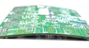
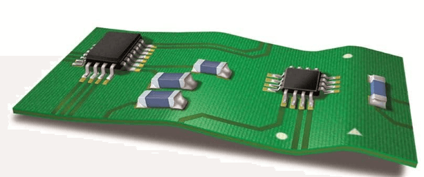
Printed Circuit Board (PCB) warping is a common manufacturing defect that occurs when the board bends or twists out of its intended flat shape. This deformation can cause significant problems in both the manufacturing process and the final product’s functionality. PCB warping affects component placement accuracy, solder joint reliability, and can even lead to complete circuit failure in severe cases.
In today’s electronics industry where components are becoming smaller and mounting densities higher, even minor PCB warping can create substantial quality issues. This comprehensive guide explores the causes of PCB warping, prevention methods during design and manufacturing, and practical techniques for repairing warped boards.
Understanding the Causes of PCB Warping
Material-Related Causes
The fundamental cause of PCB warping lies in the properties of the materials used in its construction:
- CTE Mismatch: The Coefficient of Thermal Expansion (CTE) differences between the copper layers and dielectric substrate create internal stresses when subjected to temperature changes during manufacturing or operation.
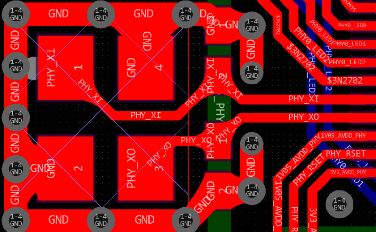
- Asymmetric Layer Stackup: Uneven copper distribution across the PCB layers leads to unbalanced stresses. For example, a board with more copper on one side than the other is prone to warping.
- Material Quality: Low-quality base materials or inconsistent prepreg (pre-impregnated fiberglass) can lead to uneven curing and subsequent warping.
Manufacturing Process Causes
Several manufacturing processes contribute to PCB warping:
- Lamination Process: Improper lamination pressure, temperature, or duration can create residual stresses in the board.
- Cooling Rate: Rapid cooling after high-temperature processes causes uneven contraction between materials.
- Copper Etching: Excessive removal of copper from one side creates imbalance in the layer structure.
- Soldering Processes: Wave soldering and reflow soldering expose the board to high temperatures that can exacerbate existing stresses.
Environmental Factors
- Moisture Absorption: Many PCB substrate materials absorb moisture from the air, which can lead to expansion and warping when heated.
- Storage Conditions: Improper storage (high humidity, temperature extremes) can affect board flatness before assembly.
- Mechanical Stress: Physical handling, mounting pressures, or enclosure constraints can induce or worsen warping.
Preventing PCB Warping During Design and Manufacturing
Design Phase Prevention
- Balanced Copper Distribution: Maintain symmetrical copper patterns across layers to balance stresses. Use copper thieving (adding non-functional copper) to balance sparse areas.
- Proper Layer Stackup: Design an even number of layers with symmetrical arrangement around the center layer. The stackup should be mirror-imaged above and below the neutral axis.
- Material Selection: Choose high-quality base materials with matched CTE properties. For high-reliability applications, consider materials like polyimide or ceramic-filled laminates that resist warping.
- Avoid Large Copper Planes: Break up large copper areas with cross-hatching or grid patterns to reduce stress concentration.
Manufacturing Process Control
- Controlled Lamination Process: Optimize lamination pressure, temperature profiles, and curing times according to material specifications.
- Gradual Cooling: Implement controlled cooling rates after high-temperature processes to allow even stress distribution.
- Baking Process: Pre-bake boards before high-temperature processes to remove moisture and stabilize the material.
- Panel Support: Use adequate support during manufacturing processes to prevent sagging or bending while the board is heated.
- Quality Inspection: Implement warpage measurement systems at critical process stages using laser scanners or shadow moiré techniques.
Methods for Repairing Warped PCBs
When prevention fails and warping occurs, several repair techniques can salvage the affected boards:
Thermal Straightening Techniques
- Controlled Heating and Weighting:
- Place the warped PCB on a flat, heat-resistant surface
- Apply gentle, even heat (typically 5-10°C below the material’s Tg)
- Place a flat weight (aluminum plate works well) on top
- Allow to cool slowly to room temperature
- Repeat if necessary with incremental temperature increases
- Hot Roller Systems:
- Specialized equipment with heated rollers that apply both heat and pressure
- Particularly effective for large panels or multiple boards
- Allows precise control of temperature and pressure profiles
- Vacuum Press Method:
- Place the board in a vacuum press between two flat plates
- Heat to just below Tg while maintaining vacuum pressure
- Hold at temperature for 15-30 minutes
- Cool slowly under pressure
Mechanical Straightening Methods
- Clamping and Baking:
- Secure the warped board in a flat clamping fixture
- Bake in an oven at 10-20°C below Tg for 1-2 hours
- Cool while maintaining clamping pressure
- Cold Pressing:
- For minor warping, use a hydraulic press with flat plates
- Apply gradual pressure over several hours
- Monitor to avoid cracking or delamination
- Stress Relief Cutting:
- For severe warping, strategic cuts in non-critical areas can relieve stress
- Requires careful planning to avoid affecting circuit functionality
- Often used in conjunction with other methods
Specialized Repair Techniques
- Selective Reflow:
- For warping caused by component soldering
- Apply localized heat to affected areas while supporting the board
- Allows solder joints to reflow and relieve stress
- Moisture Removal:
- For hygroscopic warping (caused by moisture absorption)
- Bake the board at 105-125°C for 4-12 hours
- Store in dry conditions immediately after
- Adhesive Reinforcement:
- Apply structural adhesives or stiffeners to counter warping forces
- Particularly useful for thin, flexible boards
- Must consider thermal and electrical properties of adhesives
Post-Repair Considerations
After attempting any warping repair, several important steps should follow:
- Inspection:
- Verify flatness using surface plates or optical measurement
- Check for delamination, cracks, or other damage
- Inspect critical traces and vias for integrity
- Functional Testing:
- Perform electrical testing to ensure no circuits were damaged
- Verify component alignment and solder joint quality
- Check impedance characteristics if relevant
- Preventive Measures:
- Implement proper storage conditions
- Consider conformal coating for moisture protection
- For assembled boards, ensure mounting doesn’t induce new stresses
Advanced Solutions and Emerging Technologies
The industry continues to develop new approaches to address PCB warping:
- Embedded Stress Sensors: Smart PCBs with built-in strain gauges to monitor warping in real-time.
- Adaptive Manufacturing: Machine vision systems that adjust processes based on detected warpage during production.
- Nanocomposite Materials: New substrate materials with nanoparticles that reduce CTE mismatch and improve dimensional stability.
- Shape Memory Alloys: Experimental PCBs incorporating materials that can “remember” and return to their flat shape when heated.
Conclusion
PCB warping remains a significant challenge in electronics manufacturing, but with proper understanding of its causes and implementation of preventive measures, its occurrence can be minimized. When warping does occur, the repair techniques outlined in this guide offer practical solutions ranging from simple thermal methods to advanced mechanical approaches.
The key to successful warping management lies in a comprehensive strategy that includes:
- Careful design with balanced materials and layer stackup
- Controlled manufacturing processes
- Proper handling and storage procedures
- Appropriate repair methods when needed
As electronic devices continue to evolve toward thinner, more compact designs with higher component densities, addressing PCB warping will remain critical for ensuring product quality and reliability. By applying the principles and techniques discussed here, manufacturers and repair technicians can effectively combat this persistent challenge in PCB production and maintenance.