How to Set Up Edge Conductivity in PCB Design: A Comprehensive Guide
Introduction to PCB Edge Conductivity
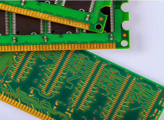
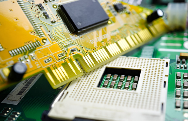
Printed Circuit Board (PCB) edge conductivity, also known as edge plating or castellation, is a specialized technique used to create electrical connections along the perimeter of a PCB. This method serves multiple purposes in electronic design, from improving EMI shielding to enabling board-to-board connections in stacked configurations.
Edge conductivity has become increasingly important in modern electronics as devices continue to shrink in size while demanding higher performance. According to industry surveys, approximately 15-20% of multilayer PCBs now incorporate some form of edge plating, with the percentage rising to nearly 35% in high-frequency and RF applications.
The process involves depositing conductive material (typically copper) along the edges of the PCB, creating a continuous conductive path that can serve various functions:
- EMI/RFI shielding for sensitive circuits
- Grounding connections between stacked boards
- Improved current carrying capacity at board edges
- Enhanced mechanical stability in edge connectors
- Heat dissipation pathways
Understanding how to properly implement edge conductivity is crucial for PCB designers working on advanced applications, particularly in telecommunications, aerospace, and high-speed computing industries where signal integrity and electromagnetic compatibility are paramount.
Methods for Implementing PCB Edge Conductivity
1. Edge Plating (Border Plating)
Edge plating is the most common method for creating conductivity along PCB edges. This process involves:
Manufacturing Process:
- Panel preparation with extended copper beyond board outline
- Routing or scoring the board to create clean edges
- Electroless copper deposition on exposed edges
- Electrolytic copper plating to build up thickness
- Optional final finishes (ENIG, HASL, etc.)
Design Requirements:
- Minimum 0.5mm copper overlap from inner layers to board edge
- Typical plating thickness of 25-35μm (1oz copper equivalent)
- Clearance of at least 1mm from edge to any non-connected features
Advantages:
- Provides 360° continuous conductivity
- Excellent for EMI shielding applications
- Creates robust edge connections
Limitations:
- Increases manufacturing complexity and cost
- Requires specific panelization techniques
- May need additional deburring steps
2. Castellations (Half-Holes)
Castellations are semi-plated through-holes placed along the board edges, creating intermittent conductive segments:
Implementation Guidelines:
- Typically 0.8-1.2mm in diameter
- Plated with standard 25μm copper minimum
- Spacing usually 1.5-2 times the hole diameter
- Often used for board-to-board soldering
Best Applications:
- Module-to-carrier board connections
- Stackable PCB designs
- Where discontinuous edge conductivity is acceptable
3. Copper Wrap-Around
This method extends internal copper layers to wrap around the board edge:
Key Parameters:
- Requires 0.3mm minimum copper extension beyond board edge
- Best for 1-2 layer boards
- Limited to straight edge segments
Typical Uses:
- Simple two-board connections
- Low-cost edge contact solutions
- Non-critical grounding applications
Design Considerations for Edge Conductivity
Electrical Considerations
Current Carrying Capacity:
- Edge plating typically carries 20-30% less current than equivalent planar traces
- For 1oz copper, safe current is approximately 3A per 10mm of plated edge
- High-current applications may require thicker plating (2-3oz)
Impedance Control:
- Edge conductivity affects board edge impedance
- Important for high-speed designs to maintain consistent impedance
- May require adjustment of dielectric spacing near edges
EMI Performance:
- Continuous edge plating provides 10-15dB better shielding than discontinuous
- Optimal when connected to ground planes at multiple points
- Gaps in plating can become slot antennas, radiating EMI
Mechanical Considerations
Board Strength:
- Edge plating increases flexural strength by 15-20%
- Helps prevent delamination in multilayer boards
- Reduces edge chipping during handling
Connector Interface:
- Gold plating (0.05-0.1μm) recommended for edge connectors
- Hard gold (cobalt-alloy) for frequent mating cycles
- Consider wear patterns in mating connector design
Thermal Effects:
- Copper edge can help dissipate heat (5-10% improvement in some cases)
- Differential thermal expansion can cause stress at corners
- May require relief cuts in high-temperature applications
Manufacturing Constraints
Fabrication Tolerances:
- Standard edge position tolerance ±0.1mm
- Plating thickness variation ±10%
- Minimum straight run length for reliable plating: 3mm
Panelization Requirements:
- Must allow for plating bus connections
- Typically requires routed tabs rather than V-scoring
- Additional clearance needed for plating fixtures
Cost Factors:
- Adds 10-25% to standard PCB cost
- Extra processing steps increase lead time
- Higher yield loss compared to standard boards
Step-by-Step Implementation Guide
1. CAD Design Phase
Layer Setup:
- Create a dedicated “Edge Plating” layer in your CAD tool
- Define plating area with 0.2mm minimum width polygon
- Connect to appropriate nets (typically ground)
Drill File Preparation:
- Include edge holes in drill file with proper notations
- Specify plated vs. non-plated holes clearly
- Add fabrication notes about edge treatment
Design Rule Checks:
- Implement specific DRC rules for edge features
- Verify clearance to non-connected copper
- Check thermal relief connections
2. Fabrication Documentation
Drawing Requirements:
- Clearly call out edge plating requirements
- Specify plating thickness and material
- Indicate any special finishes
Gerber File Notes:
- Mark edge layers as “plated” in file comments
- Include edge copper in both copper and mask layers
- Provide separate files for edge features if needed
3. Manufacturer Communication
Technical Questions:
- Confirm edge plating capabilities
- Discuss panelization approach
- Verify acceptance criteria
Special Requirements:
- Any impedance control needs
- Special finish requests
- Testing expectations
Testing and Verification Methods
Electrical Testing
Continuity Checks:
- 4-wire Kelvin measurement for low resistance
- Verify <10mΩ per 25mm of edge length
- Check isolation from adjacent nets
Current Testing:
- Apply rated current for temperature rise verification
- Should not exceed 30°C above ambient
- Measure voltage drop under load
Mechanical Testing
Adhesion Tests:
- Tape test per IPC-TM-650 2.4.1
- Cross-hatch adhesion testing
- Thermal cycling evaluation
Durability Testing:
- Mating cycle testing for edge connectors
- Wear resistance evaluation
- Environmental exposure tests
Quality Control
Visual Inspection:
- 10-40x magnification examination
- Check for plating voids or cracks
- Verify uniform plating thickness
Metallurgical Analysis:
- Cross-section microscopy
- Plating thickness measurement
- Grain structure evaluation
Common Issues and Troubleshooting
Plating Defects
Problem: Incomplete Edge Plating
- Cause: Insufficient copper wrap in design
- Solution: Increase copper overlap to 0.5mm minimum
Problem: Plating Peeling
- Cause: Poor adhesion preparation
- Solution: Specify proper surface roughening
Electrical Issues
Problem: High Resistance
- Cause: Thin or porous plating
- Solution: Specify thicker plating (2oz)
Problem: Intermittent Connections
- Cause: Contamination at edge
- Solution: Add cleaning step in process
Mechanical Problems
Problem: Edge Chipping
- Cause: Brittle plating
- Solution: Use ductile copper formulation
Problem: Connector Wear
- Cause: Insufficient gold thickness
- Solution: Specify 0.1μm hard gold
Advanced Techniques and Future Trends
High-Frequency Edge Treatments
Tapered Edge Plating:
- Gradual thickness reduction at edges
- Minimizes impedance discontinuities
- Critical for >10GHz applications
Embedded Edge Components:
- Passive components in edge structure
- Creates integrated filters
- Saves board space
Emerging Technologies
3D Printed Edge Conductors:
- Additive manufacturing approaches
- Enables complex edge geometries
- Potential for multi-material edges
Nanostructured Edge Coatings:
- Graphene-enhanced edge conductors
- Higher conductivity with less material
- Improved wear resistance
Conclusion and Best Practices
Implementing effective edge conductivity in PCB designs requires careful attention to both electrical and mechanical requirements. Based on industry experience, these best practices will help ensure success:
- Early Collaboration: Engage with your PCB manufacturer during the design phase to verify edge plating capabilities and requirements.
- Conservative Design: Allow extra margin in current ratings and mechanical tolerances for edge conductors.
- Comprehensive Documentation: Clearly specify all edge plating requirements in fabrication drawings and files.
- Prototype Testing: Always verify edge conductivity performance with physical prototypes before full production.
- Process Control: Work with manufacturers that have documented edge plating processes and quality controls.
As PCB technology continues to advance, edge conductivity techniques are becoming more sophisticated. Designers who master these techniques can create more robust, higher-performance electronic products with better EMI characteristics and more reliable interconnects. The additional effort required to properly implement edge conductivity pays dividends in product reliability and performance, particularly in demanding applications.
By following the guidelines outlined in this article and maintaining open communication with fabrication partners, engineers can effectively incorporate edge conductivity into their PCB designs while avoiding common pitfalls. The result will be higher quality boards that meet both electrical and mechanical requirements for today’s challenging applications.