How to Solve Defect Problems in PCB Manufacturing Processes
Introduction
Printed Circuit Board (PCB) manufacturing is a complex process involving multiple intricate steps, each with potential for defects that can compromise board quality and functionality. As electronic devices become more sophisticated with higher density interconnects and smaller feature sizes, the margin for error in PCB production continues to shrink. This article provides a comprehensive analysis of common PCB manufacturing defects, their root causes, and practical solutions to minimize these issues throughout the fabrication process.
Common PCB Manufacturing Defects and Solutions
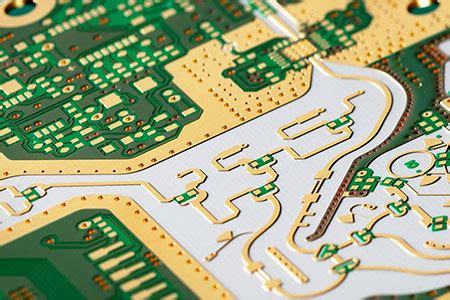
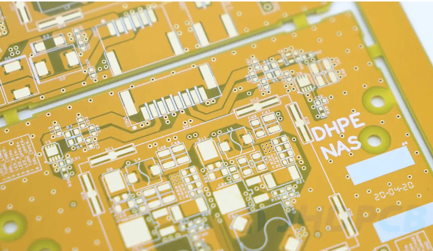
1. Copper Trace Defects
Problems:
- Open circuits (broken traces)
- Short circuits (unintended connections)
- Undercut or over-etched traces
- Inconsistent trace width
Root Causes:
- Improper etching parameters (time, temperature, solution concentration)
- Photoresist application issues
- Copper plating problems
- Mechanical stress during handling
Solutions:
- Implement strict process controls for etching (monitor and adjust etchant composition regularly)
- Use advanced direct imaging systems for more accurate pattern transfer
- Adopt additive processes rather than subtractive etching where appropriate
- Implement automated optical inspection (AOI) after etching to catch defects early
- Use proper handling procedures and fixtures to prevent mechanical damage
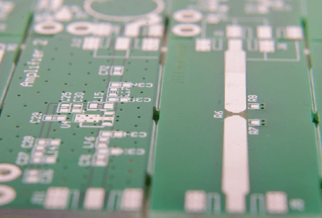
2. Solder Mask Issues
Problems:
- Incomplete coverage (pinholes, voids)
- Misregistration (alignment errors)
- Poor adhesion
- Uneven thickness
Root Causes:
- Contamination on copper surface
- Improper cleaning before application
- Incorrect exposure or development parameters
- Low-quality solder mask material
Solutions:
- Implement rigorous cleaning processes (chemical and mechanical)
- Use plasma treatment before solder mask application to improve adhesion
- Standardize application methods (curtain coating, spray coating, or screen printing)
- Optimize exposure energy and development time through DOE (Design of Experiments)
- Implement automatic optical inspection after solder mask application
3. Drilling-Related Defects
Problems:
- Hole wall roughness
- Smear (resin residue in holes)
- Drill breakage
- Inaccurate hole placement
- Barrel cracking
Root Causes:
- Worn or improper drill bits
- Incorrect drill parameters (speed, feed rate)
- Improper material support during drilling
- Inadequate chip removal
Solutions:
- Implement predictive drill bit replacement schedules
- Use advanced drill bit materials (carbide with special coatings)
- Optimize drill parameters for specific material stacks
- Implement vacuum systems for effective chip removal
- Use laser drilling for microvias and high-density applications
- Conduct regular spindle maintenance and calibration
4. Plating Defects
Problems:
- Voids in plated through holes
- Uneven plating thickness
- Poor adhesion of plating
- “Dog-boning” at via entrances
Root Causes:
- Inadequate hole cleaning/desmear
- Poor activation of hole walls
- Incorrect plating bath chemistry
- Improper current density distribution
Solutions:
- Implement optimized desmear processes (chemical and plasma)
- Use reverse pulse plating for more uniform deposition
- Regular bath analysis and maintenance
- Implement agitation and filtration systems
- Use conformal anodes for better current distribution
- Conduct cross-sectioning for process validation
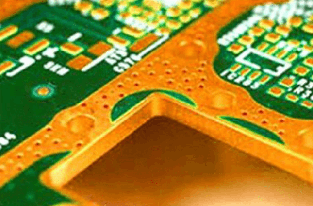
5. Lamination Defects
Problems:
- Delamination
- Voids or bubbles
- Resin starvation
- Warpage
Root Causes:
- Contamination between layers
- Improper lamination pressure/temperature profiles
- Moisture absorption in materials
- CTE (Coefficient of Thermal Expansion) mismatches
Solutions:
- Implement strict cleanliness protocols
- Pre-bake materials to remove moisture
- Optimize lamination cycle through testing
- Use matched CTE materials in stackup
- Implement slow ramp rates for temperature changes
- Use vacuum lamination systems
6. Surface Finish Defects
Problems:
- Oxidation
- Uneven deposition
- Whisker growth (especially with tin)
- Poor solderability
Root Causes:
- Contamination before finishing
- Improper chemical bath maintenance
- Inadequate thickness
- Storage conditions
Solutions:
- Implement proper cleaning before surface finishing
- Regular bath analysis and maintenance
- Use ENIG (Electroless Nickel Immersion Gold) or other high-reliability finishes
- Control storage environment (temperature, humidity)
- Implement shelf-life controls for sensitive finishes
Process Improvement Methodologies
1. Statistical Process Control (SPC)
Implement SPC techniques to monitor critical parameters and detect process variations before they result in defects. This includes:
- Control charts for key parameters (thickness, hole size, etc.)
- Process capability analysis (Cp, Cpk)
- Trend analysis to predict maintenance needs
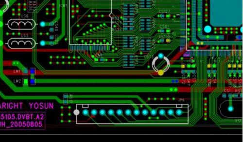
2. Design for Manufacturability (DFM)
Collaborate with design engineers to ensure PCB designs are optimized for manufacturing:
- Appropriate trace/space rules
- Proper via sizing and placement
- Consideration of material capabilities
- Panelization considerations
3. Advanced Process Monitoring
Implement real-time monitoring systems:
- Automated optical inspection (AOI)
- X-ray inspection for inner layers and BGAs
- Impedance testing for high-speed designs
- Flying probe testing for electrical continuity
4. Root Cause Analysis and Corrective Action
When defects occur, implement structured problem-solving:
- Fishbone diagrams to identify potential causes
- 5 Whys analysis to get to root causes
- FMEA (Failure Mode and Effects Analysis) to anticipate potential failures
- Implement permanent corrective actions rather than temporary fixes
5. Employee Training and Certification
Invest in comprehensive training programs:
- Process-specific training for operators
- Certification programs for critical processes
- Cross-training to improve process understanding
- Regular refresher courses
Emerging Technologies for Defect Reduction
1. Industry 4.0 and Smart Manufacturing
- IoT sensors for real-time process monitoring
- Machine learning algorithms for defect prediction
- Digital twins for process optimization
- Automated adjustment of process parameters
2. Advanced Materials
- High-reliability substrate materials
- Improved solder mask formulations
- Nanocoating for better surface protection
- Low-loss materials for high-frequency applications
3. Precision Manufacturing Technologies
- Laser direct imaging for finer features
- Additive manufacturing approaches
- Advanced plasma processing
- High-precision registration systems
Conclusion
Reducing defects in PCB manufacturing requires a comprehensive approach that addresses materials, processes, equipment, and human factors. By understanding the root causes of common defects and implementing systematic solutions, manufacturers can significantly improve yield and product reliability. The most effective strategies combine rigorous process control with advanced monitoring technologies and continuous improvement methodologies. As PCB technology continues to advance with finer features and more complex architectures, maintaining low defect rates will require ongoing investment in both technology and workforce development. Manufacturers who adopt these best practices will be positioned to deliver high-quality PCBs consistently while minimizing waste and rework.