How to Understand Proper PCB Handling Procedures
At work, I ensure that assembled PCBs avoid these types of errors. With hundreds of tiny components soldered onto them, PCBs are less robust than you might imagine. If handled improperly, you risk complaints from unhappy system installers whose circuits may not function properly.
Should PCB Designers Be Concerned About PCB Handling?
Odds are, you’re not likely to have hundreds of PCBs manufactured from your design. The people who will come into contact with these PCBs are assemblers, test engineers, installers, and maintenance personnel.
The fact that you won’t be involved in the post-production process doesn’t mean you can be complacent about PCB handling. It’s important to understand the proper PCB handling procedures; failure to do so could lead to circuit failure.
More importantly, PCB designers should be aware of their role in optimizing PCB layouts to minimize issues related to PCB handling. The last thing you want is to rework an existing PCB when you’re supposed to be tackling your next project.
How Improper PCB Handling Can Cause Damage
Given the choice, I’d rather deal with damaged porcelain than deal with problems caused by improper PCB handling. While the former is obvious, the damage caused by PCB handling issues is often negligible. There are often no obvious signs until a PCB stops functioning properly after installation.
A common problem observed when PCBs are handled carelessly is the failure of active components due to electrostatic discharge (ESD). This occurs when PCBs are handled in a non-ESD-safe environment. For ESD-sensitive components, less than 3,000 volts are required to cause real damage to their internal circuitry.
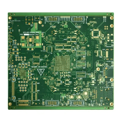
If you look closely at a reflow-soldered PCB, you’ll notice that only a very small amount of solder holds the surface-mount (SMD) components to their pads. When mechanical force is applied parallel to the PCB, components such as SMD capacitors can have one of their pads break off.
In other words, when you try to pick up a PCB with one hand, you press the PCB against itself. This can cause the PCB to bend slightly and potentially dislodge certain components from their pads. To avoid this, it’s a good idea to pick up the PCB with two hands.
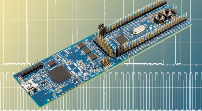
Improper handling of PCBs can cause electronic devices to malfunction.
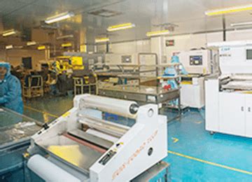
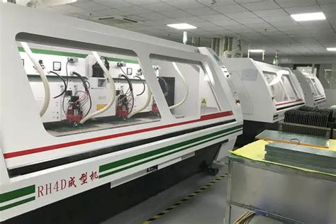
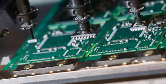
PCBs are often panelized to reduce costs and increase efficiency. After assembly, the PCBs need to be disassembled. Even if they are supported by a minimum V rating, some force is still required to separate them. This process can also accidentally damage the solder joints of certain components.
While uncommon, sometimes carelessness can cause you to drop a PCB like a porcelain bowl. The sudden impact can damage larger components, such as electrolytic capacitors, or even damage the pads.
Design Techniques to Reduce PCB Handling Issues
PCB designers are not completely helpless when dealing with PCB handling issues. Implementing the right design strategies can, to a certain extent, help minimize defects related to PCB handling.
Electrostatic Discharge Protection
To prevent sensitive components from failing due to ESD, you need to add protective components to suppress transients during electrostatic discharge. Varistors and Zener diodes are commonly used to handle the rapid discharge of ESD. In addition, there are specialized ESD protection devices that can provide better protection against such phenomena.
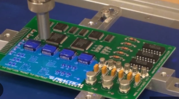
ESD protection is crucial when handling PCBs.
Component Placement
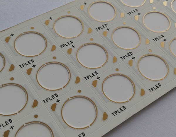
You can’t prevent PCBs from mechanical stress. However, you can mitigate such issues by ensuring that components are placed appropriately. For example, you know that placing SMD capacitors against the damaging forces applied during the depanelization process increases the risk of solder cracking.
Therefore, you need to place SMD capacitors or similar components parallel to the fold line to minimize the impact of the applied force. In addition, avoid placing components close to the curvature or bend line of the PCB and avoid placing components close to the outline of the board.