How to Use Different Colors to Highlight Different Nets in PCB Design
Introduction to PCB Net Highlighting
Printed Circuit Board (PCB) design is a complex process that requires careful attention to electrical connections between components. One of the most valuable visualization tools in PCB design software is the ability to highlight different nets (electrical connections) using distinct colors. This technique, often called “net highlighting” or “net coloring,” provides designers with immediate visual feedback about the routing status and connectivity of their board.
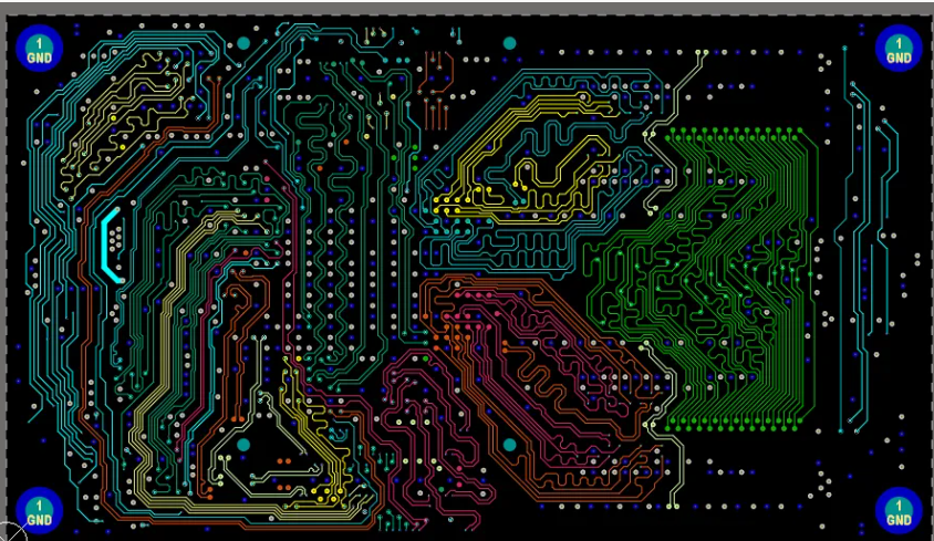
When working with complex PCB designs containing hundreds or thousands of connections, the standard rat’s nest display (the mass of crisscrossing lines showing unconnected routes) can become overwhelmingly confusing. By assigning different colors to different nets, designers can:
- Quickly identify specific signals in a crowded layout
- Track routing progress for critical nets
- Visually separate power, ground, and signal layers
- Highlight differential pairs or matched-length groups
- Troubleshoot connectivity issues more efficiently
Understanding PCB Design Software Capabilities
Most modern PCB design tools support net coloring functionality, though the specific implementation varies between software packages. Some of the most popular PCB design applications include:
Altium Designer
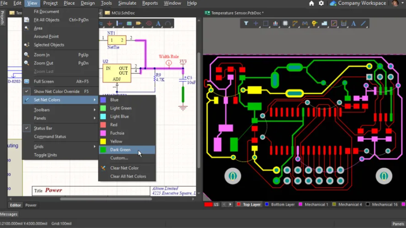
Altium provides robust net highlighting capabilities through its “PCB” panel. Designers can:
- Assign colors to individual nets or net classes
- Save color schemes as presets
- Toggle between colored view and standard view
- Adjust highlight intensity
KiCad
In KiCad’s PCBNew editor:
- Use the “Highlight Net” tool (shortcut ‘~’)
- Right-click on a net to change its color
- Configure persistent highlighting in display options
- Set different colors for ratsnest and routed traces
Eagle
Autodesk Eagle offers:
- Net coloring through the “RATSNEST” command
- Layer-specific coloring options
- Ability to highlight airwires (unrouted connections) separately
OrCAD/Allegro
Cadence’s solutions provide:
- Comprehensive net color management
- Group highlighting for buses and differential pairs
- 3D visualization with maintained net colors
Step-by-Step Guide to Assigning Net Colors
1. Preparing Your Design for Net Coloring
Before assigning colors, ensure your schematic and PCB are properly synchronized:
- Verify all components are correctly linked between schematic and layout
- Confirm your netlist is up to date
- Check that no design rule violations exist that might affect net connectivity
2. Accessing Net Management Tools
Locate your software’s net management panel:
- In Altium: View » Panels » PCB
- In KiCad: Tools » Net Inspector
- In Eagle: Edit » Net Classes
- In OrCAD: Setup » Colors
3. Selecting Nets for Coloring
Choose which nets to color based on:
- Signal type (power, ground, high-speed, etc.)
- Functional grouping (USB, HDMI, memory bus)
- Routing priority (critical timing nets first)
- Layer assignment (different colors per layer)
4. Assigning Colors to Nets
The actual coloring process typically involves:
- Selecting the net from a list
- Choosing a color from a palette
- Applying the color to:
- Ratsnest (unrouted connections)
- Routed traces
- Vias and pads
- Both
5. Saving Color Schemes
Create and save color presets for:
- Different design phases (placement, routing, verification)
- Various board sections (power supply, analog, digital)
- Team collaboration standards
Advanced Net Coloring Techniques
Differential Pair Coloring
For high-speed designs, assign complementary colors to:
- Positive and negative legs of differential pairs
- Matched-length groups
- Clock signals and their associated grounds
Power Distribution Coloring
Use a graduated color scheme to visualize:
- Voltage levels (red for higher, blue for lower)
- Current capacity (brighter colors for higher current)
- Power domains (distinct colors for each domain)
Signal Integrity Visualization
Color coding can help identify:
- Impedance-controlled traces
- Length-matched groups
- Crosstalk-prone areas
Layer-Specific Coloring
Combine net colors with layer colors to:
- Quickly identify layer transitions
- Visualize via placement
- Balance layer utilization
Best Practices for Effective Net Coloring
Color Selection Guidelines
- Use high-contrast colors for important nets
- Reserve bright colors (red, yellow) for critical signals
- Use darker colors for less important connections
- Maintain consistency across projects
Organizational Strategies
- Create a color legend document
- Standardize colors for common signals (red for power, blue for ground)
- Use similar hues for related signals
- Implement team-wide color standards
Performance Considerations
- Limit the number of colored nets in large designs
- Disable coloring when not needed to improve rendering performance
- Use simpler coloring modes during intensive editing
Troubleshooting Common Issues
Color Visibility Problems
If colors aren’t appearing as expected:
- Check layer visibility settings
- Verify that highlighting is enabled
- Adjust background contrast
- Confirm color override permissions
Performance Slowdowns
For laggy performance with coloring:
- Reduce the number of highlighted nets
- Lower highlight intensity
- Disable anti-aliasing
- Update graphics drivers
Inconsistent Colors Between Team Members
To maintain color consistency:
- Share color preset files
- Document color assignments
- Use version-controlled design templates
- Standardize monitor calibration
Practical Applications of Net Coloring
Design Review Process
Use colored nets to:
- Quickly communicate routing status
- Identify incomplete connections
- Highlight areas needing attention
- Demonstrate signal flow to stakeholders
Debugging and Rework
Colored nets help with:
- Tracing signal paths during debugging
- Identifying incorrect connections
- Planning rework modifications
- Verifying fixes
Documentation and Presentation
Enhanced visuals for:
- Design presentations
- Manufacturing instructions
- Assembly documentation
- Training materials
Future Trends in PCB Visualization
AI-Assisted Net Coloring
Emerging technologies may offer:
- Automatic color assignment based on net characteristics
- Dynamic coloring that responds to design changes
- Predictive highlighting of potential problem areas
Augmented Reality Integration
Future applications could include:
- AR overlays with colored net visualization
- 3D board inspection with maintained net colors
- Interactive design reviews with net highlighting
Enhanced Collaboration Features
Potential developments:
- Real-time shared coloring in cloud-based tools
- Version-controlled color schemes
- Commenting tied to colored nets
Conclusion
Effective use of color in PCB net highlighting is more than just an aesthetic choice—it’s a powerful productivity tool that can significantly enhance your design workflow. By strategically assigning colors to different nets, you can transform an overwhelming tangle of connections into a clearly organized visual representation of your circuit.
The techniques discussed in this article—from basic single-net highlighting to advanced layer-specific coloring schemes—provide a foundation for developing your own effective visualization strategies. Remember that the optimal approach varies depending on your specific design requirements, team dynamics, and personal preferences.
As PCB designs continue growing in complexity, the ability to quickly identify and track individual connections becomes increasingly valuable. Mastering net coloring techniques will help you work more efficiently, reduce errors, and communicate your design intent more clearly throughout the product development process.
Whether you’re a beginner learning your first PCB tool or an experienced designer looking to optimize your workflow, investing time in developing effective net coloring practices will pay dividends throughout your design career. Start implementing these techniques in your next project and experience the immediate benefits of clearer, more organized PCB visualization.