How to Use Printed Circuit Boards (PCBs): A Comprehensive Guide
Introduction to Printed Circuit Boards
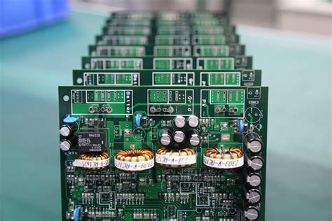
Printed Circuit Boards (PCBs) form the foundation of modern electronics, serving as the physical platform that connects and supports various electronic components in virtually all electronic devices we use today. From smartphones and computers to medical equipment and automotive systems, PCBs enable the complex functionality we’ve come to depend on in our technological world.
A PCB is a flat board made of insulating material (typically fiberglass) with conductive pathways—usually made of copper—etched or printed onto its surface. These pathways, called traces, electrically connect different components mounted on the board, replacing the need for complex wiring systems that were common in early electronic devices.
Understanding how to properly use PCBs is essential for electronics engineers, hobbyists, and technicians alike. This comprehensive guide will walk you through the fundamental aspects of working with printed circuit boards, from basic handling to advanced implementation techniques.
Understanding PCB Basics
Types of PCBs
Before using a PCB, it’s important to recognize the different types available:
- Single-sided PCBs: The simplest type, with copper traces on only one side of the insulating substrate.
- Double-sided PCBs: Feature conductive layers on both sides, connected by vias (plated-through holes).
- Multi-layer PCBs: Contain three or more conductive layers, used in complex electronics like smartphones and computers.
- Flexible PCBs: Made with flexible materials that can bend, useful in wearable devices and compact electronics.
- Rigid-Flex PCBs: Combine rigid and flexible sections for specialized applications.
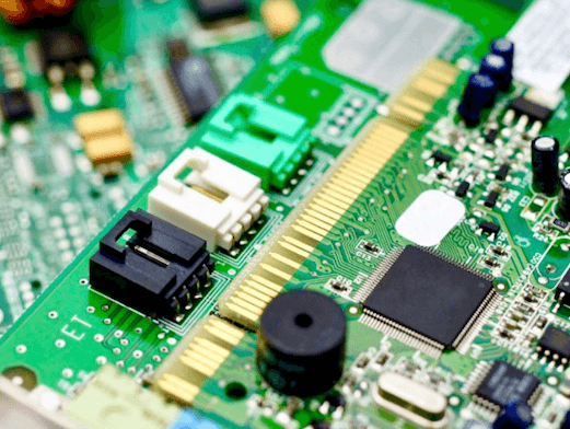
PCB Components
A typical PCB consists of several key elements:
- Substrate: The base insulating material (usually FR-4 fiberglass)
- Copper layers: Conductive pathways for electrical signals
- Solder mask: Protective layer that prevents short circuits
- Silkscreen: Printed labels and identifiers for components
- Pads: Connection points for component leads
- Vias: Conductive holes that connect different layers
Preparing to Use a PCB
1. PCB Handling and Safety
Proper handling is crucial when working with PCBs:
- Always handle PCBs by their edges to avoid contaminating contact surfaces
- Wear anti-static wrist straps when working with sensitive components
- Store PCBs in anti-static bags when not in use
- Work in a clean, well-lit area free from dust and moisture
- Avoid touching gold-plated connectors with bare hands to prevent corrosion
2. Necessary Tools and Equipment
To effectively work with PCBs, you’ll need:
- Soldering iron (temperature-controlled preferred)
- Solder wire (lead-free or leaded, depending on application)
- Flux and flux cleaner
- Tweezers and precision pliers
- Wire cutters
- Magnifying glass or microscope for inspection
- Multimeter for testing
- Desoldering tools (solder wick, desoldering pump)
- PCB holder or vise to secure the board during work
PCB Assembly Process
1. Component Placement
The first step in using a PCB is placing the electronic components:
- Study the schematic and PCB layout: Understand where each component belongs
- Start with the lowest-profile components: Typically resistors, diodes, and small capacitors
- Progress to taller components: Such as electrolytic capacitors and connectors
- Place ICs last: Especially important for surface-mount devices (SMDs)
- Double-check orientation: Many components like diodes, electrolytic capacitors, and ICs have polarity that must be observed
For surface-mount technology (SMT) components:
- Use tweezers for precise placement
- Apply a small amount of solder paste to pads before placement
- Consider using a stencil for precise solder paste application in production
2. Soldering Techniques
Proper soldering is essential for reliable PCB operation:
Through-hole soldering:
- Insert the component leads through the appropriate holes
- Bend the leads slightly to hold the component in place
- Heat the pad and component lead simultaneously with the soldering iron
- Apply solder to the joint, not directly to the iron
- Allow the joint to cool naturally
- Trim excess leads after soldering
Surface-mount soldering:
- Apply flux to the pads
- Place a small amount of solder on one pad
- While heating the solder, position the component with tweezers
- Solder the opposite side to fully secure the component
- Go back and reflow the initial joint if needed
Hot air rework station:
- Essential for multi-pin SMD components
- Apply flux to the component area
- Use appropriate nozzle size for the component
- Maintain consistent movement to avoid overheating
- Allow proper cooling time before handling
3. Inspection and Testing
After assembly, thorough inspection is crucial:
- Visual inspection:
- Check for solder bridges between pins
- Verify all components are properly placed and oriented
- Look for cold solder joints (dull, grainy appearance)
- Ensure no excess flux residue remains
- Continuity testing:
- Use a multimeter to check for proper connections
- Verify no shorts exist where they shouldn’t
- Test power and ground planes for proper connectivity
- Power-up testing:
- Initially use current-limited power supply
- Check for overheating components
- Verify basic functionality before full operation
PCB Implementation in Projects
1. Mounting the PCB
Proper mounting ensures mechanical stability:
- Use standoffs to prevent the PCB from touching metal surfaces
- Select appropriate screw sizes to avoid damaging the board
- Consider vibration dampening in high-vibration environments
- Allow adequate space for heat dissipation if needed
2. Connecting External Components
Many PCBs require external connections:
- Use appropriate connectors for the application (USB, terminal blocks, etc.)
- Consider strain relief for cables that may experience pulling
- Keep signal and power cables separated when possible
- Use shielded cables for sensitive signals
3. Power Considerations
Proper power delivery is essential:
- Verify voltage requirements before connecting power
- Consider adding fuses or poly switches for protection
- Ensure adequate current capacity for all components
- Implement proper decoupling with capacitors near ICs
Troubleshooting Common PCB Issues
Even with careful assembly, issues may arise:
- Short circuits:
- Visually inspect for solder bridges
- Use a multimeter in continuity mode to locate shorts
- Check for conductive debris or whiskers
- Open circuits:
- Verify all connections with continuity testing
- Check for broken traces or damaged vias
- Inspect for cold solder joints
- Intermittent connections:
- Look for hairline cracks in traces
- Check for poorly formed solder joints
- Verify connector seating
- Component failures:
- Check for overheating signs
- Verify proper orientation of polarized components
- Test components individually when possible.
Advanced PCB Usage Techniques
1. Working with Multi-layer Boards
Multi-layer PCBs require special consideration:
- Be aware of internal planes (power and ground)
- Understand via types (through, blind, buried)
- Consider layer stack-up when designing or modifying
- Use appropriate tools for debugging (oscilloscopes, logic analyzers)
2. PCB Modification and Rework
Sometimes modifications are necessary:
- Trace repairs: Use jumper wires for broken traces
- Component replacement: Proper desoldering techniques are essential
- Adding components: Verify compatibility with existing circuit
- Cutting traces: Use exacto knife carefully to isolate circuits
3. Environmental Considerations
PCBs may need special treatment in certain environments:
- High humidity: Use conformal coating
- High temperature: Select appropriate components and materials
- Vibration: Additional mechanical support may be needed
- Outdoor use: UV-resistant materials and proper sealing
Best Practices for PCB Usage
To ensure optimal performance and longevity:
- Thermal management:
- Provide adequate ventilation
- Use heat sinks for power components
- Consider thermal vias in high-heat areas
- Signal integrity:
- Keep high-speed signals short
- Use proper grounding techniques
- Implement impedance matching where needed
- Maintenance:
- Periodically inspect for dust accumulation
- Check for corroded contacts in harsh environments
- Verify connector integrity over time
- Documentation:
- Keep schematics and layout diagrams accessible
- Document any modifications made
- Maintain a record of component specifications
Future Trends in PCB Technology
As electronics continue to evolve, so do PCBs:
- Higher density interconnects: Finer traces and smaller vias
- Embedded components: Passive components within the PCB layers
- Flexible hybrid electronics: Combining rigid and flexible technologies
- 3D printed electronics: Additive manufacturing of circuits
- Advanced materials: High-frequency and thermal-conductive substrates
Conclusion
Printed Circuit Boards are the backbone of modern electronics, and understanding how to properly use them is an essential skill for anyone working with electronic systems. From careful handling and proper assembly techniques to troubleshooting and advanced implementation, each step in the PCB usage process contributes to the reliability and performance of the final product.
By following the guidelines outlined in this comprehensive guide—paying attention to proper soldering techniques, thorough inspection processes, and appropriate implementation methods—you can ensure successful PCB usage in your projects. Whether you’re a professional engineer or an electronics hobbyist, mastering PCB usage will enable you to bring your electronic designs to life with confidence and precision.
Remember that PCB technology continues to advance, so maintaining up-to-date knowledge and skills will be crucial for working with next-generation circuit boards. With practice and attention to detail, you’ll be able to harness the full potential of printed circuit boards in all your electronic endeavors.


