How to Write Text on a PCB: Techniques and Best Practices
Introduction to PCB Text
Printed Circuit Boards (PCBs) often require text markings for various purposes, including component identification, version numbers, company logos, and instructional information. These markings serve critical functions in assembly, testing, debugging, and maintenance of electronic devices. Unlike ordinary printing, PCB text must withstand harsh manufacturing processes and environmental conditions while maintaining clarity and precision.
This comprehensive guide explores the various methods for adding text to PCBs, covering design considerations, manufacturing techniques, and practical recommendations for creating effective, durable markings on your circuit boards.
Why Add Text to PCBs?
Before examining the how, it’s important to understand why text is added to PCBs:
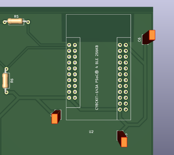
- Component Identification: Labels for components (R1, C5, U3) help during assembly and debugging
- Polarity Indicators: Marks showing proper orientation of components
- Version Control: Board revision numbers and dates
- Regulatory Compliance: Safety certifications and compliance marks
- Manufacturer Information: Company names, logos, and copyrights
- Test Points: Identification of test and measurement locations
- Instructional Text: Warnings, handling instructions, or interface labels
PCB Text as Part of the Design
1. Silkscreen Layer (Legend Printing)
The most common method for adding text to PCBs is through the silkscreen layer, also known as the legend printing. This is typically a white epoxy ink (though other colors are possible) applied to the board’s surface.
Design Considerations:
- Minimum recommended line width: 0.15mm (6mil)
- Minimum character height: 1.0mm for readability
- Font selection: Simple sans-serif fonts work best (Arial, Verdana)
- Avoid placing text over holes or pads
- Maintain clearance from solderable areas (typically 0.2mm)
Pros:
- Cost-effective
- Good readability
- Multiple color options
- Works well for most applications
Cons:
- Limited resolution for very small text
- Can be damaged by abrasion or chemicals
- Not suitable for extremely harsh environments
2. Copper Text (Etched Lettering)
Text can be incorporated into the copper layers of the PCB, either as part of the signal layers or in dedicated copper layers for markings.
Implementation Methods:
- Positive Text: Copper remains where text appears
- Negative Text: Copper is removed to form text (requires plating)
Design Tips:
- Minimum width: 0.1mm (4mil) for reliable etching
- Consider text orientation relative to etching process
- Account for copper weight when designing line widths
Advantages:
- Extremely durable
- Can be plated with solder, gold, or other finishes
- No additional printing process required
- Works well for EMI shielding applications
Disadvantages:
- Lower contrast than silkscreen
- More limited design flexibility
- Requires careful design to avoid signal interference
3. Solder Mask Text
Text can be created by exposing the copper through the solder mask in the shape of letters.
Key Characteristics:
- Text appears as the color of the exposed copper or plating
- Typically used for small, high-precision markings
- Requires precise alignment during manufacturing
Best Practices:
- Minimum line width: 0.1mm (4mil)
- Works best with simple fonts
- Avoid very large text areas that might affect soldering
Advanced PCB Text Techniques
4. Laser Marking
For high-precision or specialized applications, laser marking offers excellent results.
Types of Laser Marking:
- Laser Engraving: Removes material to create contrast
- Laser Annealing: Changes surface properties without material removal
- Carbonization: Creates dark marks on certain substrates
Benefits:
- Extremely high precision (up to 0.02mm resolution)
- No physical contact with the board
- Permanent marking
- Can mark on uneven surfaces
- Ideal for serial numbers and barcodes
Limitations:
- Higher cost than silkscreening
- Requires specialized equipment
- Limited color options (typically black or dark marks)
5. Inkjet Printing
Modern inkjet technology allows for direct printing on PCBs with specialized inks.
Features:
- Full color capability
- No screens or phototools needed
- Good for prototyping and low-volume production
- Can print variable data (serial numbers, dates)
Considerations:
- Ink durability may be less than traditional methods
- Surface preparation is critical
- Limited to certain substrate types
6. Embossed/Debossed Text
Physical text can be created by modifying the PCB substrate itself.
Implementation Options:
- Embossing: Raised lettering
- Debossing: Indented lettering
- Typically done during the pressing process
Use Cases:
- Tactile indicators for blind operation
- Extreme environment applications
- When all other marking methods are unsuitable
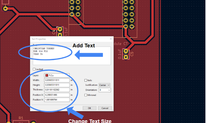
Design Guidelines for PCB Text
Font Selection and Sizing
- Standard Fonts: Stick to simple, sans-serif fonts like Arial or Verdana
- Minimum Sizes:
- General purpose: 1.0mm height
- High-density boards: 0.5mm height (with appropriate line width)
- Aspect Ratio: Maintain stroke width at least 15% of character height
- Spacing: Letter spacing should be at least 0.15mm
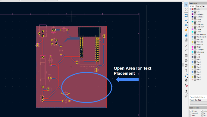
Placement Considerations
- Avoid Critical Areas:
- Keep text away from solderable surfaces
- Don’t place over vias or holes
- Maintain clearance from board edges
- Orientation:
- Standard reading direction (left-to-right for most languages)
- Consistent alignment throughout the board
- Layer Selection:
- Top layer for component-side markings
- Bottom layer for solder-side markings
- Inner layers only when necessary
Internationalization
- Language Selection: Use English or internationally recognized symbols
- Symbols vs. Text: Consider using standardized symbols when possible
- Localization Requirements: Check target market regulations
Manufacturing Considerations
Design for Manufacturing (DFM)
- Consult Your Fabricator: Get their specific capabilities and limitations
- Color Contrast: Ensure sufficient contrast between text and background
- Process Compatibility: Verify text method works with all board finishes
- Testing Requirements: Ensure text won’t interfere with test fixtures
Cost Factors
- Number of Colors: Each additional silkscreen color adds cost
- Special Processes: Laser marking, inkjet, etc., may have premium pricing
- Board Complexity: High-density designs may require more expensive text methods
- Volume Considerations: Some methods have high setup costs but low per-unit costs
Special Applications
1. High-Density Interconnect (HDI) Boards
For HDI designs with very small features:
- Use laser marking for tiny text
- Consider copper text for permanence
- Minimum sizes may need to be reduced
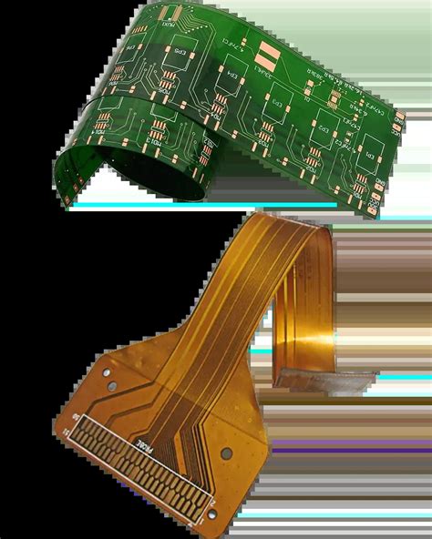
2. Flexible PCBs
Special considerations for flex circuits:
- Ink adhesion is critical
- Laser marking may affect flexibility
- Text must withstand bending
3. High-Reliability Applications
For military, aerospace, or medical applications:
- Extreme durability requirements
- Often mandate specific marking methods
- May require special verification processes
Troubleshooting Common PCB Text Issues
Problem: Faint or Incomplete Text
Possible Causes:
- Insufficient line width in design
- Manufacturing process limitations
- Ink viscosity problems
Solutions:
- Increase text stroke width
- Consult with manufacturer about process capabilities
- Consider alternative marking methods
Problem: Text Wears Off Easily
Possible Causes:
- Poor ink adhesion
- Insufficient curing
- Abrasive handling
Solutions:
- Specify higher-quality inks
- Add protective coating
- Change text method (e.g., to laser marking)
Problem: Text Misalignment
Possible Causes:
- Registration issues during manufacturing
- Board warpage
- Design errors
Solutions:
- Add alignment marks
- Review manufacturing tolerances
- Adjust design to account for process variations
Future Trends in PCB Text
- Smart Markings: QR codes and barcodes for traceability
- Nanoscale Text: For ultra-high density applications
- Dynamic Markings: Using e-ink or similar technologies
- Augmented Reality Integration: Marks designed for AR interpretation
- Environmentally Friendly Inks: Bio-based or low-VOC options
Conclusion
Adding text to PCBs is a critical aspect of board design that serves both practical and regulatory purposes. The appropriate method depends on your specific requirements for durability, resolution, color, and cost. Silkscreening remains the most common approach for general applications, while copper text and laser marking offer solutions for more demanding environments.
By understanding the various options and following design best practices, you can ensure your PCB markings are clear, durable, and effective throughout the product lifecycle. Always consult with your manufacturing partner early in the design process to verify their specific capabilities and limitations regarding text implementation.
Remember that good PCB text design contributes significantly to the manufacturability, usability, and serviceability of your electronic products. Invest the necessary time and attention to get it right, and your future self (and everyone else who handles your boards) will thank you.