If you want to design a good PCB, the substrate process is indispensable
If you want to design a good PCB, the substrate process is indispensable
The basic design process of general PCB is as follows:
Preliminary preparation → PCB structure design → guide netlist → rule setting → PCB layout → wiring → wiring optimization and silk screen → network and DRC inspection and structure inspection → output photo-drawing → photo-drawing review → PCB board production/proofing data → PCB board factory engineering EQ confirmation → patch data output → project completion.
1: Preliminary preparation
This includes preparing package libraries and schematics. Before designing PCB, you must first prepare the logic package of the schematic SCH and the package library of the PCB. The package library can be the library that comes with PADS, but it is generally difficult to find a suitable one. It is best to make your own package library based on the standard size data of the selected device. In principle, make the package library of PCB first, and then make the logic package of SCH. The package library of PCB has higher requirements, which directly affects the installation of the board; the logic package of SCH has relatively loose requirements, as long as you pay attention to defining the pin attributes and the corresponding relationship with the PCB package. PS: Pay attention to the hidden pins in the standard library. After that, it is the design of the schematic, and after it is done, you are ready to start PCB design.
2: PCB structure design
This step is to draw the PCB surface in the PCB design environment according to the determined circuit board size and various mechanical positioning, and place the required connectors, buttons/switches, screw holes, assembly holes, etc. according to the positioning requirements. And fully consider and determine the wiring area and non-wiring area (such as how much area around the screw hole belongs to the non-wiring area).
3: Netlist
It is recommended to import the board frame before the netlist. Import the board frame in DXF format or emn format
4: Rule setting
Reasonable rules can be set according to the specific PCB design. The rules we are talking about are the constraint manager of PADS. Through the constraint manager, the line width and safety spacing are constrained at any link in the design process. The places that do not meet the constraints will be marked with DRC Markers during the subsequent DRC detection.
Generally, the rule setting is placed before the layout, because sometimes some fanout work needs to be completed during the layout, so the rules should be set before the fanout. When the design project is large, the design can be completed more efficiently. Note: Setting rules is to complete the design better and faster, in other words, to facilitate the designer. The general settings are: 1. Default line width/line spacing for common signals. 2. Select and set vias. 3. Line width and color settings for important signals and power supplies. 4. Board layer settings
5: PCB layout
Generally, the layout is carried out according to the following principles:
(1) Reasonable division according to electrical performance, generally divided into: digital circuit area (i.e. afraid of interference and generates interference), analog circuit area (afraid of interference), power drive area (interference source);
(2) Circuits that complete the same function should be placed as close as possible, and the components should be adjusted to ensure the simplest connection; at the same time, the relative positions of the functional blocks should be adjusted to make the connection between the functional blocks as simple as possible;
(3) For components with large mass, the installation position and installation strength should be considered; heating components should be placed separately from temperature-sensitive components, and thermal convection measures should be considered if necessary;
(4) I/O driver devices should be as close to the edge of the printed circuit board as possible and close to the lead-out connectors;
(5) Clock generators (such as crystal oscillators or clock oscillators) should be as close as possible to the devices that use the clock;
(6) A decoupling capacitor (generally a monolithic capacitor with good high-frequency performance) should be added between the power input pin and the ground of each integrated circuit; when the circuit board space is dense, a tantalum capacitor can also be added around several integrated circuits.
(7) A discharge diode (1N4148 is sufficient) should be added to the relay coil;
(8) The layout should be balanced, orderly and dense, and should not be top-heavy or one-sided. Special attention should be paid to the placement of components. The actual size (area and height) of the components and the relative position between the components should be considered to ensure the electrical performance of the circuit board and the feasibility and convenience of production and installation. At the same time, the placement of the components should be appropriately modified to make them neat and beautiful, while ensuring that the above principles can be reflected. For example, the same components should be placed neatly and in the same direction, and should not be placed “staggered”. This step is related to the overall image of the board and the difficulty of the next wiring, so it is necessary to spend a lot of effort to consider it. When laying out, preliminary wiring can be done for places that are not sure, and full consideration should be given.
6: Wiring
Wiring is the most important process in the entire PCB design. This will directly affect the performance of the PCB board. In the design process of the PCB, wiring is generally divided into three levels:
The first is wiring, which is the most basic requirement for PCB design. If the wiring is not connected and there are flying wires everywhere, it will be an unqualified board and it can be said that it has not yet entered the market.
The second is the satisfaction of electrical performance. This is the standard for measuring whether a printed circuit board is qualified. This is after the wiring is connected, carefully adjust the wiring to achieve the best electrical performance. The next is aesthetics. If your wiring is connected and there is no place that affects the electrical performance, but it looks messy and colorful at first glance, then no matter how good your electrical performance is, it will still be rubbish in the eyes of others. This will cause great inconvenience to testing and maintenance. The wiring should be neat and uniform, and should not be criss-crossed and disorderly. All of this must be achieved while ensuring the electrical performance and meeting other individual requirements, otherwise it will be a waste of effort.
The wiring is mainly carried out according to the following principles:
(1) In general, the power line and ground line should be wired first to ensure the electrical performance of the circuit board. Within the scope of conditions, try to widen the width of the power supply and ground wires. It is best that the ground wire is wider than the power supply wire. The relationship between them is: ground wire > power supply wire > signal wire. Usually the signal wire width is: 0.2~0.3mm (about 8-12mil), and the thinnest width can reach 0.05~0.07mm (2-3mil). The power line is generally 1.2~2.5mm (50-100mil). For the PCB of digital circuits, a wide ground wire can be used to form a loop, that is, to form a ground network for use (the ground of analog circuits cannot be used in this way).
(2) Pre-wire the wires with stricter requirements (such as high-frequency wires). The edge wires of the input and output ends should avoid being adjacent and parallel to avoid reflection interference. If necessary, ground wire isolation should be added. The wiring of two adjacent layers should be perpendicular to each other. Parallel wiring is prone to parasitic coupling.
(3) The oscillator shell is grounded, and the clock line should be as short as possible and cannot be led everywhere. Under the clock oscillator circuit and special high-speed logic circuit, the ground area should be increased, and other signal lines should not be routed, so that the surrounding electric field approaches zero;
(4) Use 45° zigzag wiring as much as possible, and do not use 90° zigzag wiring to reduce the radiation of high-frequency signals; (Lines with high requirements should also use double arcs)
(5) No signal line should form a loop. If it is unavoidable, the loop should be as small as possible; the vias of the signal line should be as few as possible;
(6) The key lines should be as short and thick as possible, and protective ground should be added on both sides.
(7) When transmitting sensitive signals and noise field band signals through flat cables, the “ground wire-signal-ground wire” method should be used to lead them out.
(8) Test points should be reserved for key signals to facilitate production and maintenance inspection.
(9) After the schematic wiring is completed, the wiring should be optimized; at the same time, after the preliminary network check and DRC check are correct, the ground wire is filled in the unwired area, and a large area of copper layer is used as the ground wire. On the printed circuit board, all unused areas are connected to the ground as ground wires. Or make a multi-layer board, with the power supply and ground wires occupying one layer each. PCB wiring process requirements (can be set in the rules)
(1) Line In general, the signal line width is 0.3mm (12mil), and the power line width is 0.77mm (30mil) or 1.27mm (50mil); the distance between lines and between lines and pads is greater than or equal to 0.33mm (13mil). In actual applications, if conditions permit, consider increasing the distance; When the wiring density is high, you can consider (but not recommend) using two lines between IC pins, the line width is 0.254mm (10mil), and the line spacing is not less than 0.254mm (10mil). In special cases, when the device pins are dense and the width is narrow, the line width and line spacing can be appropriately reduced.
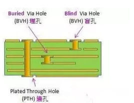
(2) Pads (PADs) The basic requirements for pads (PADs) and transition holes (VIAs) are: the diameter of the pad should be larger than the diameter of the hole by 0.6mm; for example, general pin-type resistors, capacitors and integrated circuits use pad/hole sizes of 1.6mm/0.8mm (63mil/32mil), and sockets, pins and diodes 1N4007 use 1.8mm/1.0mm (71mil/39mil). In actual applications, the pad size should be determined according to the actual size of the component. If conditions permit, the pad size can be appropriately increased; the component mounting hole diameter designed on the PCB board should be about 0.2 to 0.4mm (8-16mil) larger than the actual size of the component pin.
(3) Vias (VIAs) Generally 1.27mm/0.7mm (50mil/28mil); When the wiring density is high, the via size can be appropriately reduced, but it should not be too small. You can consider using 1.0mm/0.6mm (40mil/24mil). (4) Spacing requirements for pads, lines, and vias PAD and VIA: ≥ 0.3mm (12mil) PAD and PAD: ≥ 0.3mm (12mil) PAD and TRACK: ≥ 0.3mm (12mil) TRACK and TRACK: ≥ 0.3mm (12mil) When the density is high: PAD and VIA: ≥ 0.254mm (10mil) PAD and PAD: ≥ 0.254mm (10mil) PAD and TRACK: ≥ 0.254mm (10mil) TRACK and TRACK: ≥ 0.254mm (10mil)
7: Wiring optimization and silk screen
“There is no best, only better”! No matter how hard you think about the design, after you finish drawing and take a look, you will still find that many places can be modified. The general design experience is: the time to optimize the wiring is twice the time for the first wiring. After you feel that there is nothing to modify, you can lay copper. Copper is usually laid for ground wires (note the separation of analog ground and digital ground), and it may also be necessary to lay power for multi-layer boards. When it comes to silk screen printing, be careful not to be blocked by devices or removed by vias and pads. At the same time, when designing, look directly at the component surface, and the bottom layer of words should be mirrored to avoid confusing the layers.
8: Network, DRC inspection and structural inspection
Before light painting, it is generally necessary to check. Each company will have its own Check List, which includes requirements for various links such as principle, design, and production. The following is an introduction from the two main inspection functions provided by the software. DRC inspection:
9: Output light painting
Before light painting output, it is necessary to ensure that the single board is the latest version that has been completed and meets the design requirements. The light painting output files are used for board making by the board factory, steel mesh making by the steel mesh factory, and process files made by the welding factory.
The output files are (taking a four-layer board as an example):
1). Wiring layer: refers to the conventional signal layer, mainly wiring. Named L1, L2, L3, L4, where L represents the layer of the routing layer.
2). Silkscreen layer: refers to the layer in the design file that provides information for processing silkscreen. Usually, when there are devices or logos on both the top and bottom layers, there will be top and bottom silkscreens. Naming: The top layer is named SILK_TOP; the bottom layer is named SILK_BOTTOM.
3). Solder mask layer: refers to the layer in the design file that provides processing information for green oil coating. Naming: The top layer is named SOLD_TOP; the bottom layer is named SOLD_BOTTOM.
4). Steel mesh layer: refers to the layer in the design file that provides processing information for solder paste coating. Usually, when there are SMD devices on both the top and bottom layers, there will be steel mesh top and steel mesh bottom. Naming: The top layer is named PASTE_TOP; the bottom layer is named PASTE_BOTTOM.
5). Drilling layer (including 2 files, NC DRILL numerical control drilling file and DRILL DRAWING drilling diagram) named NC DRILL and DRILL DRAWING respectively.
10: Photolithography review
After outputting the photolithography, photolithography inspection and Cam350 open and short circuit inspections must be carried out before sending it to the board factory for board making. In the later stage, attention must be paid to the board making project and problem response.
11: PCB board making data (Gerber photolithography data + PCB board making requirements + puzzle board diagram)
12: PCB board factory engineering EQ confirmation (board making project and problem response).
13: PCBA patch data output (steel mesh data, patch number map, component coordinate file).
At this point, all the PCB design workflows for a project are completed
PCB design is a very meticulous job, so you must be extremely careful and patient when designing, and fully consider all factors, including production, assembly and processing, and later maintenance. In addition, developing some good working habits during design will make your design more reasonable, more efficient, easier to produce, and better in performance. When good designs are applied to daily products, consumers will feel more assured and trustful.