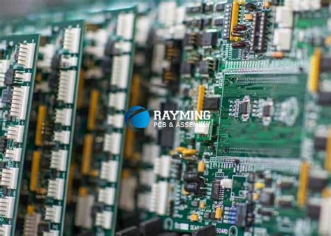
Impedance control in pcb manufacturing
Understanding Impedance Control In PCB Design
Impedance control in printed circuit board (PCB) design is a critical aspect that ensures the reliable performance of electronic devices. As electronic systems become increasingly complex and operate at higher frequencies, the need for precise impedance control becomes paramount.
Impedance, in the context of PCB design, refers to the resistance encountered by an alternating current as it travels through the circuit.
This resistance is not merely a function of the conductive material but also depends on the frequency of the signal, the geometry of the traces, and the dielectric properties of the materials used.
To understand the importance of impedance control, it is essential to consider the role of signal integrity in electronic devices.
Signal integrity refers to the preservation of the quality of electrical signals as they traverse the PCB. Poor signal integrity can lead to data loss, increased error rates, and overall system unreliability. Impedance mismatches are a primary cause of signal integrity issues, as they can result in signal reflections, distortions, and attenuation. Therefore, maintaining consistent impedance throughout the PCB is crucial for minimizing these adverse effects.
Achieving impedance control involves careful consideration of several design parameters.
The width and thickness of the copper traces, the spacing between them, and the dielectric constant of the substrate material all influence the impedance. Designers often use simulation tools to model the impedance characteristics of their PCB layouts, allowing them to make necessary adjustments before fabrication. These tools can predict how changes in trace dimensions or material properties will affect the impedance, enabling designers to optimize their designs for specific applications.
Moreover, the choice of materials plays a significant role in impedance control.
The dielectric constant of the substrate material affects the capacitance between traces, which in turn influences the impedance. Materials with a stable dielectric constant over a range of frequencies are preferred, as they provide more predictable impedance characteristics. Additionally, the use of controlled dielectric materials can help achieve tighter impedance tolerances, which is particularly important for high-frequency applications.
Manufacturing processes also impact impedance control. Variations in etching, lamination, and plating processes can lead to deviations from the intended trace dimensions, affecting the impedance.
Therefore, manufacturers must adhere to stringent process controls and quality assurance measures to ensure that the fabricated PCBs meet the specified impedance requirements. This often involves the use of advanced fabrication techniques and equipment capable of maintaining tight tolerances.
Furthermore, testing and verification are integral to ensuring impedance control in PCB manufacturing.
Impedance measurements are typically conducted using time-domain reflectometry (TDR) or vector network analyzers (VNA) to verify that the manufactured PCBs conform to the design specifications. These tests help identify any discrepancies that may have arisen during fabrication, allowing for corrective actions to be taken before the PCBs are deployed in electronic systems.
In conclusion, impedance control is a fundamental aspect of PCB design that directly impacts the performance and reliability of electronic devices. By understanding the factors that influence impedance and employing rigorous design, manufacturing, and testing practices, designers and manufacturers can ensure that their PCBs meet the demanding requirements of modern electronic applications. As technology continues to advance, the importance of precise impedance control will only grow, underscoring its critical role in the development of next-generation electronic systems.

Techniques For Achieving Precise Impedance Control
In the realm of printed circuit board (PCB) manufacturing, achieving precise impedance control is a critical aspect that ensures the optimal performance of electronic devices. Impedance, which is the measure of opposition that a circuit presents to the flow of alternating current, must be meticulously controlled to maintain signal integrity, especially in high-frequency applications. As electronic devices become increasingly complex, the demand for precise impedance control has grown, necessitating the adoption of advanced techniques in PCB manufacturing.
One of the primary techniques for achieving precise impedance control is the careful design of the PCB stack-up.
The stack-up refers to the arrangement of the various layers of a PCB, including the conductive and dielectric layers. By strategically selecting the materials and thicknesses of these layers, manufacturers can influence the impedance of the traces. For instance, using materials with a low dielectric constant can help reduce signal loss and maintain consistent impedance levels. Additionally, the thickness of the dielectric layers can be adjusted to fine-tune the impedance, allowing for greater control over the electrical characteristics of the board.
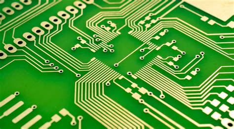
Another crucial technique involves the precise control of trace geometry.
The width and spacing of the traces on a PCB have a significant impact on impedance. By employing advanced computer-aided design (CAD) tools, manufacturers can simulate and optimize trace dimensions to achieve the desired impedance levels.
These tools allow for the accurate modeling of electromagnetic fields, enabling designers to predict how changes in trace geometry will affect impedance. Furthermore, the use of controlled impedance traces, such as microstrip and stripline configurations, can help maintain consistent impedance across the board, reducing the risk of signal reflection and distortion.
In addition to stack-up design and trace geometry, the choice of materials plays a pivotal role in impedance control. High-frequency PCBs often require specialized materials that offer low dielectric loss and stable electrical properties over a wide range of frequencies.
Materials such as polytetrafluoroethylene (PTFE) and ceramic-filled laminates are commonly used in these applications due to their excellent dielectric properties. By selecting the appropriate materials, manufacturers can ensure that the PCB maintains its impedance characteristics even under varying environmental conditions.
Moreover, the manufacturing process itself must be tightly controlled to achieve precise impedance.
This includes maintaining strict tolerances during the etching and lamination processes to ensure that the physical dimensions of the traces and layers remain consistent with the design specifications.
Advanced manufacturing techniques, such as laser direct imaging and precision drilling, can help achieve the high level of accuracy required for impedance-controlled PCBs. These techniques allow for the creation of fine features and complex geometries that are essential for maintaining impedance control in modern electronic devices.
Finally, thorough testing and validation are essential to ensure that the manufactured PCBs meet the desired impedance specifications.
Techniques such as time-domain reflectometry (TDR) and vector network analysis (VNA) are commonly used to measure the impedance of the traces and identify any discrepancies from the design. By conducting rigorous testing, manufacturers can verify that the PCB will perform as intended in its final application, providing confidence in the reliability and performance of the electronic device.
In conclusion, achieving precise impedance control in PCB manufacturing requires a multifaceted approach that encompasses careful design, material selection, manufacturing precision, and thorough testing. As electronic devices continue to evolve, the importance of these techniques will only grow, underscoring the need for ongoing innovation and refinement in the field of PCB manufacturing.
The Role Of Materials In Impedance Control
In the realm of printed circuit board (PCB) manufacturing, impedance control is a critical factor that ensures the reliable performance of electronic devices. Impedance, which is the measure of opposition that a circuit presents to the flow of alternating current, must be meticulously managed to maintain signal integrity, especially in high-frequency applications. The role of materials in achieving precise impedance control cannot be overstated, as they significantly influence the electrical properties of the PCB.
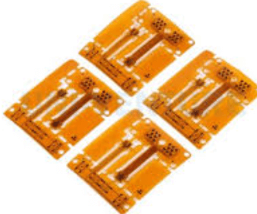
To begin with, the choice of substrate material is paramount in determining the impedance characteristics of a PCB.
The substrate, typically made from a dielectric material, serves as the foundation upon which the circuit is built. Common materials include FR-4, a glass-reinforced epoxy laminate, and more advanced options like Rogers or Teflon-based laminates. Each of these materials possesses distinct dielectric constants and loss tangents, which directly affect the impedance. For instance, a higher dielectric constant can lead to lower impedance, which may be desirable or undesirable depending on the specific application. Therefore, selecting the appropriate substrate material is crucial for achieving the desired impedance levels.
Moreover, the copper traces that form the conductive pathways on a PCB also play a significant role in impedance control.
The thickness and width of these traces, along with the spacing between them, are critical parameters that influence impedance. Thicker traces tend to have lower resistance, which can reduce impedance, while narrower traces can increase it. Additionally, the surface roughness of the copper can impact the skin effect, where high-frequency signals travel primarily on the surface of the conductor, thus affecting impedance. Manufacturers must carefully control these physical dimensions and properties to ensure that the impedance remains within specified limits.
Transitioning to the role of solder mask and other protective coatings, these materials can also impact impedance.
The solder mask, which is applied over the copper traces to protect them from oxidation and environmental damage, can alter the effective dielectric constant of the PCB. This change can, in turn, affect the impedance. Therefore, the choice of solder mask material and its thickness must be considered in the impedance control strategy. Similarly, any additional coatings or finishes applied to the PCB, such as conformal coatings, can influence the overall impedance and must be accounted for during the design phase.
Furthermore, the manufacturing process itself can introduce variations in material properties that affect impedance.
For example, the lamination process, which involves bonding multiple layers of material together under heat and pressure, can lead to variations in dielectric constant and thickness. These variations can result in impedance mismatches, which can degrade signal integrity. Consequently, manufacturers must implement stringent quality control measures to minimize these variations and ensure consistent impedance across production batches.
In conclusion, the role of materials in impedance control during PCB manufacturing is multifaceted and complex. From the selection of substrate materials to the precise control of copper trace dimensions and the impact of protective coatings, each aspect must be carefully managed to achieve the desired impedance characteristics. As electronic devices continue to evolve and demand higher performance, the importance of understanding and controlling these material properties will only grow, underscoring the need for ongoing research and innovation in this critical area of PCB manufacturing.

Common Challenges In Impedance Control And How To Overcome Them
Impedance control in PCB manufacturing is a critical aspect that ensures the reliable performance of electronic circuits, particularly in high-frequency applications.
However, achieving precise impedance control presents several challenges that manufacturers must address to maintain the integrity and functionality of the final product.
One of the primary challenges in impedance control is the variability in material properties.
The dielectric constant and thickness of the substrate material can significantly influence the impedance of a trace. Variations in these properties, even within the same batch of materials, can lead to inconsistencies in impedance values. To overcome this, manufacturers can implement stringent quality control measures and work closely with material suppliers to ensure consistency. Additionally, using advanced simulation tools during the design phase can help predict and compensate for potential variations.
Another challenge arises from the manufacturing process itself.
The etching process, which defines the width and spacing of the copper traces, can introduce variations that affect impedance.
Over-etching or under-etching can alter the trace dimensions, leading to deviations from the intended impedance values.
To mitigate this, manufacturers can employ precise etching techniques and regularly calibrate their equipment to maintain accuracy.
Furthermore, incorporating design for manufacturability (DFM) principles can help in anticipating and minimizing these variations during the design stage.
The complexity of modern PCB designs also contributes to impedance control challenges.
As circuits become more intricate, with multiple layers and varying trace geometries, maintaining consistent impedance across all traces becomes increasingly difficult. This complexity necessitates a comprehensive understanding of electromagnetic theory and the use of sophisticated design software that can model and simulate the entire PCB stack-up. By leveraging these tools, designers can optimize trace layouts and layer configurations to achieve the desired impedance characteristics.
Moreover, environmental factors such as temperature and humidity can impact impedance.
These factors can cause the dielectric properties of the substrate to change, leading to impedance drift. To address this, manufacturers can select materials with stable dielectric properties over a wide range of environmental conditions. Additionally, implementing robust testing procedures that simulate real-world operating conditions can help identify potential issues before the PCB is deployed.
Communication between design and manufacturing teams is another crucial element in overcoming impedance control challenges.
Often, discrepancies arise due to a lack of understanding or miscommunication between these teams. Establishing clear communication channels and fostering a collaborative environment can ensure that design specifications are accurately translated into the manufacturing process. Regular meetings and design reviews can facilitate this collaboration, allowing for the early identification and resolution of potential issues.
Finally, continuous education and training for engineers and technicians involved in PCB manufacturing are essential.
As technology evolves, staying updated with the latest advancements in materials, processes, and design techniques is crucial for maintaining effective impedance control. Investing in training programs and encouraging knowledge sharing within the organization can enhance the skill set of the workforce, ultimately leading to improved manufacturing outcomes.
In conclusion, while impedance control in PCB manufacturing presents several challenges, these can be effectively managed through a combination of material consistency, precise manufacturing processes, advanced design tools, environmental considerations, effective communication, and continuous education. By addressing these areas, manufacturers can ensure that their PCBs meet the stringent performance requirements of modern electronic applications.