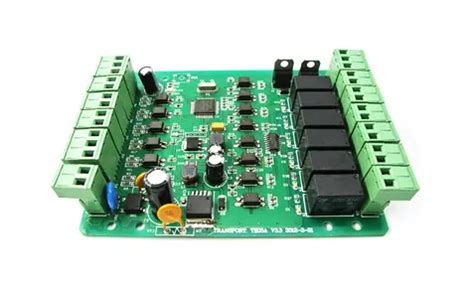
Improve the level of PCB wiring to make your PCB design more efficient
Improve the level of PCB wiring to make your PCB design more efficient
PCB wiring is very important in the entire PCB design. How to achieve fast and efficient wiring and make your PCB wiring look tall and grand is worth studying. 7 aspects that need to be paid attention to in PCB wiring are sorted out. Come and check for omissions!
1.Common ground processing of digital circuits and analog circuits
Nowadays, many PCBs are no longer single-function circuits (digital or analog circuits), but are composed of a mixture of digital circuits and analog circuits. Therefore, when wiring, it is necessary to consider the mutual interference between them, especially the noise interference on the ground line. The frequency of digital circuits is high and the sensitivity of analog circuits is strong. For signal lines, high-frequency signal lines should be as far away from sensitive analog circuit devices as possible. For ground lines, the entire PCB has only one node to the outside world, so the problem of digital and analog common ground must be processed inside the PCB. In fact, the digital ground and analog ground are separated inside the board. They are not connected to each other, but only at the interface where the PCB is connected to the outside world (such as plugs, etc.). There is a short circuit between the digital ground and the analog ground. Please note that there is only one connection point. There are also some that do not share the same ground on the PCB, which is determined by the system design.
2.Signal lines are laid on the electrical (ground) layer
When wiring a multi-layer printed circuit board, since there are not many lines left in the signal line layer, adding more layers will cause waste and increase the workload of production, and the cost will increase accordingly. To solve this contradiction, you can consider wiring on the electrical (ground) layer. First, you should consider using the power layer, and then the ground layer. Because it is best to preserve the integrity of the ground layer.
3.Treatment of connecting legs in large-area conductors
In large-area grounding (electricity), the legs of common components are connected to it. The treatment of connecting legs needs to be comprehensively considered. In terms of electrical performance, it is better for the pads of the component legs to be fully connected to the copper surface, but there are some bad hidden dangers for the welding and assembly of components, such as: ① Welding requires a high-power heater. ② It is easy to cause cold solder joints. Therefore, taking into account both electrical performance and process requirements, a cross-shaped pad is made, which is called heat shield, commonly known as thermal pad. In this way, the possibility of producing cold solder joints due to excessive heat dissipation in the cross section during welding can be greatly reduced. The treatment of the power (ground) layer legs of multilayer boards is the same.
4.The role of the network system in wiring
In many CAD systems, wiring is determined by the network system. If the grid is too dense, the number of pathways will increase, but the step is too small, and the amount of data in the drawing field is too large, which will inevitably have higher requirements for the storage space of the equipment, and also have a great impact on the computing speed of computer-related electronic products. Some pathways are invalid, such as those occupied by the pads of the component legs or by the mounting holes and fixed holes. If the grid is too sparse, too few pathways will have a great impact on the wiring rate. Therefore, a reasonable grid system should be available to support the wiring. The distance between the two legs of a standard component is 0.1 inch (2.54 mm), so the basis of the grid system is generally set to 0.1 inch (2.54 mm) or an integer multiple of less than 0.1 inch, such as: 0.05 inch, 0.025 inch, 0.02 inch, etc.
5.Processing of power and ground wires
Even if the wiring in the entire PCB board is completed well, the interference caused by the lack of consideration of the power and ground wires will reduce the performance of the product and sometimes even affect the success rate of the product. Therefore, the wiring of the power and ground wires should be taken seriously, and the noise interference generated by the power and ground wires should be reduced to a minimum to ensure the quality of the product. For every engineer engaged in the design of electronic products, they understand the cause of the noise between the ground wire and the power wire. Now only the reduction method of noise suppression is described: it is well known that a decoupling capacitor is added between the power and ground wires. Try to widen the width of the power supply and ground wires. It is best that the ground wire is wider than the power supply wire. The relationship between them is: ground wire>power line>signal line. Usually the signal line width is: 0.2~0.3mm, the finest width can reach 0.05~0.07mm, and the power line is 1.2~2.5 mm. For the PCB of digital circuits, a wide ground wire can be used to form a loop, that is, to form a ground network for use (the ground of analog circuits cannot be used in this way). Use a large area of copper layer as a ground wire, and connect all unused areas on the printed circuit board to the ground as a ground wire. Or make a multi-layer board, with the power supply and ground wire occupying one layer each.

6.Design Rule Check (DRC)
After the wiring design is completed, it is necessary to carefully check whether the wiring design conforms to the rules set by the designer, and also to confirm whether the rules set conform to the requirements of the printed circuit board production process.
The general inspection includes the following aspects: whether the distance between lines, lines and component pads, lines and through holes, component pads and through holes, and through holes is reasonable and meets the production requirements.
Is the width of the power line and the ground line appropriate?
Is the power and ground line tightly coupled (low wave impedance)?
Is there any place in the PCB where the ground line can be widened? Have the best measures been taken for the key signal lines, such as the shortest length, adding protection lines, and the input and output lines are clearly separated. Do the analog circuits and digital circuits have their own independent ground lines? Will the graphics (such as icons and annotations) added to the PCB later cause signal short circuits? Modify some undesirable line shapes. Are there process lines added to the PCB?
Does the solder mask meet the requirements of the production process? Is the solder mask size appropriate? Is the character logo pressed on the device pad to avoid affecting the quality of the electrical equipment. Whether the outer frame edge of the power ground layer in the multilayer board is reduced. If the copper foil of the power ground layer is exposed outside the board, it is easy to cause a short circuit.
7.Design of vias
Via is one of the important components of multilayer PCBs. The cost of drilling holes usually accounts for 30% to 40% of the cost of PCB board manufacturing. Simply put, every hole on the PCB can be called a via. From the perspective of function, vias can be divided into two categories: one is used as an electrical connection between layers; the other is used to fix or position devices. If from the perspective of process technology, vias are generally divided into three categories, namely blind vias, buried vias and through vias.
Blind vias are located on the top and bottom surfaces of printed circuit boards, with a certain depth, and are used to connect the surface circuits and the inner circuits below. The depth of the hole usually does not exceed a certain ratio (aperture).
Buried vias refer to connection holes located in the inner layer of printed circuit boards, which do not extend to the surface of the circuit board. The above two types of holes are located in the inner layer of the circuit board. They are completed by the through-hole forming process before lamination.
During the process of forming the through-hole, several inner layers may be overlapped. The third type is called a through-hole. This hole passes through the entire circuit board and can be used to achieve internal interconnection or as a component installation positioning hole. Since through-holes are easier to implement in terms of process and have lower costs, they are used in most printed circuit boards instead of the other two types of vias.
The vias mentioned below are considered as through-holes unless otherwise specified.
1.From a design perspective, a via is mainly composed of two parts, one is the drill hole in the middle, and the other is the pad area around the drill hole. The size of these two parts determines the size of the via. Obviously, in high-speed and high-density PCB design, designers always hope that the vias are as small as possible, so that more wiring space can be left on the board.
2.In addition, the smaller the via, the smaller its own parasitic capacitance is, and it is more suitable for high-speed circuits. However, the reduction of hole size also brings about an increase in cost, and the size of the via cannot be reduced indefinitely. It is limited by process technologies such as drilling and plating: the smaller the hole, the longer it takes to drill, and the easier it is to deviate from the center position; and when the depth of the hole exceeds 6 times the diameter of the drill hole, it is impossible to ensure that the hole wall can be evenly copper plated. For example, the thickness (through hole depth) of a normal 6-layer PCB board is about 50Mil, so the minimum drilling diameter that PCB manufacturers can provide can only reach 8Mil.
3.Parasitic capacitance of vias The via itself has parasitic capacitance to the ground. If it is known that the diameter of the isolation hole of the via on the ground layer is D2, the diameter of the via pad is D1, the thickness of the PCB board is T, and the dielectric constant of the board substrate is ε, then the parasitic capacitance of the via is approximately: C=1.41εTD1/(D2-D1) The parasitic capacitance of the via will mainly affect the circuit by extending the rise time of the signal and reducing the speed of the circuit.
4.For example, for a PCB board with a thickness of 50 mil, if a via with an inner diameter of 10 mil and a pad diameter of 20 mil is used, and the distance between the pad and the ground copper area is 32 mil, we can use the above formula to approximate the parasitic capacitance of the via: C = 1.41×4.4×0.050×0.020/(0.032-0.020) = 0.517pF, and the rise time change caused by this part of the capacitance is: T10-90 = 2.2C (Z0/2) = 2.2×0.517x (55/2) = 31.28ps. From these values, it can be seen that although the effect of the rise delay caused by the parasitic capacitance of a single via is not very obvious, if the via is used multiple times in the routing to switch between layers, the designer should still consider it carefully.
5.Parasitic inductance of vias Similarly, vias have parasitic capacitance and parasitic inductance. In the design of high-speed digital circuits, the harm caused by parasitic inductance of vias is often greater than the influence of parasitic capacitance.
Its parasitic series inductance will weaken the contribution of bypass capacitance and weaken the filtering effect of the entire power supply system. We can use the following formula to simply calculate the approximate parasitic inductance of a via: L=5.08h[ln(4h/d)+1] where L refers to the inductance of the via, h is the length of the via, and d is the diameter of the center drill hole. It can be seen from the formula that the diameter of the via has little effect on the inductance, while the length of the via has the greatest impact on the inductance. Still using the above example, the inductance of the via can be calculated as: L=5.08×0.050[ln(4×0.050/0.010)+1]=1.015nH. If the rise time of the signal is 1ns, then its equivalent impedance is: XL=πL/T10-90=3.19Ω. Such impedance can no longer be ignored when there is a high-frequency current passing through. In particular, it should be noted that the bypass capacitor needs to pass through two vias when connecting the power layer and the ground layer, so the parasitic inductance of the via will increase exponentially.
6. Via Design in High-Speed PCB Through the above analysis of the parasitic characteristics of vias, we can see that in high-speed PCB design, seemingly simple vias often bring great negative effects to the design of the circuit. In order to reduce the adverse effects of the parasitic effects of vias, the following can be done as much as possible in the design:
- Considering both cost and signal quality, choose a reasonable size of via. For example, for the 6-10 layer memory module PCB design, it is better to use 10/20Mil (drilling/pad) vias. For some high-density small-sized boards, you can also try to use 8/18Mil vias. Under current technical conditions, it is difficult to use smaller vias. For vias of power or ground, you can consider using a larger size to reduce impedance.
- The two formulas discussed above show that using a thinner PCB board is conducive to reducing the two parasitic parameters of vias.
- Try not to change layers for signal routing on the PCB board, that is, try not to use unnecessary vias.
- The pins of power and ground should be drilled nearby, and the leads between the vias and the pins should be as short as possible, because they will increase inductance. At the same time, the leads of power and ground should be as thick as possible to reduce impedance.
- Place some grounded vias near the vias where the signal changes layers to provide the closest loop for the signal. You can even place a large number of redundant ground vias on the PCB board. Of course, you also need to be flexible and changeable when designing. The via model discussed above is the case where each layer has a pad. Sometimes, we can reduce or even remove the pads of certain layers. Especially when the via density is very high, it may cause a broken groove to form in the copper layer, which will cut off the circuit. To solve this problem, in addition to moving the position of the via, we can also consider reducing the pad size of the via in the copper layer.