Inductors on PCB: Design, Implementation, and Applications
Introduction
Inductors are fundamental passive components in electronic circuits, storing energy in a magnetic field when current flows through them. On printed circuit boards (PCBs), inductors play a crucial role in power supply circuits, signal filtering, RF applications, and impedance matching. Integrating inductors into PCB designs requires careful consideration of factors such as inductance value, current handling, parasitic effects, and physical layout. This article explores the types of PCB inductors, their design considerations, implementation techniques, and common applications.
Types of Inductors Used in PCBs
1. Wire-Wound Inductors
- Constructed by winding conductive wire (usually copper) around a core (air, ferrite, or powdered iron).
- Offers high inductance and current-handling capability.
- Common in power supply circuits and high-frequency applications.
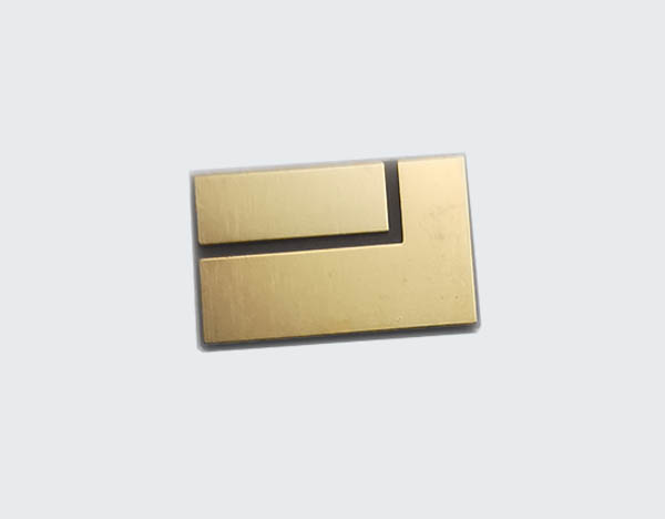
2. Multilayer Chip Inductors
- Surface-mount device (SMD) inductors built using layered ferrite or ceramic materials.
- Compact and suitable for high-frequency applications like RF circuits.
- Low profile makes them ideal for space-constrained designs.
3. Planar Inductors
- Fabricated directly on the PCB using spiral or meander-shaped traces.
- Eliminates the need for discrete components, reducing cost and size.
- Used in high-frequency circuits, such as wireless communication modules.
4. Toroidal Inductors
- Ring-shaped cores with wire windings, providing high inductance with minimal electromagnetic interference (EMI).
- Often used in power electronics and noise-filtering applications.
5. Thin-Film Inductors
- Deposited on a substrate using thin-film technology, enabling precise inductance values.
- Common in high-frequency and microwave applications.
Design Considerations for PCB Inductors
1. Inductance Value
- The required inductance depends on the application (e.g., power filtering, RF matching).
- Calculated using formulas or simulation tools (e.g., ANSYS, COMSOL).
2. Current Rating
- Inductors must handle the maximum expected current without saturation.
- Wire thickness and core material affect current capacity.
3. Parasitic Effects
- Parasitic capacitance: Occurs between windings, affecting high-frequency performance.
- DC resistance (DCR): Causes power loss and heating.
- Skin effect: At high frequencies, current flows near the conductor surface, increasing resistance.
4. Core Material Selection
- Air-core: Low loss, suitable for high-frequency applications.
- Ferrite-core: High permeability, used for power inductors.
- Iron-powder core: Balances inductance and saturation current.
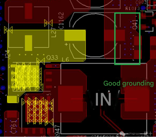
5. PCB Layout Considerations
- Trace width: Wider traces reduce resistance and improve current handling.
- Spacing between turns: Minimizes parasitic capacitance.
- Ground plane effects: A nearby ground plane can alter inductance due to eddy currents.
Implementing Inductors on PCBs
1. Discrete Inductor Placement
- SMD inductors are soldered onto pads, following manufacturer guidelines.
- Ensure proper thermal management to avoid overheating.
2. PCB Trace Inductors (Planar Inductors)
- Spiral or meander patterns etched into copper layers.
- Inductance depends on trace width, spacing, and number of turns.
- Example: A square spiral inductor can be modeled using the formula:
[
L \approx \mu_0 n^2 d_{avg} \left[ \ln\left(\frac{2.46}{\phi}\right) + 0.20 \phi^2 \right]
]
where: - (L) = inductance (H),
- (n) = number of turns,
- (d_{avg}) = average diameter,
- (\phi) = fill ratio.
3. Multilayer Inductors
- Stacked spirals on different PCB layers increase inductance.
- Requires careful via placement to minimize parasitic resistance.
4. Shielding and EMI Mitigation
- Use ground planes or ferrite shields to reduce electromagnetic interference.
- Keep high-frequency inductors away from sensitive analog circuits.
Applications of PCB Inductors
1. Power Supply Circuits
- Buck/boost converters: Store and transfer energy in switching regulators.
- LC filters: Smooth output voltage ripple.
2. RF and Wireless Communication
- Impedance matching: Ensures maximum power transfer in antennas.
- Resonant circuits: Used in oscillators and filters.
3. Signal Integrity and Filtering
- EMI suppression: Choke inductors block high-frequency noise.
- Differential mode filtering: Reduces noise in high-speed data lines.
4. High-Frequency and Microwave Circuits
- MMICs (Monolithic Microwave Integrated Circuits): Thin-film inductors enable miniaturization.
- RFIDs and IoT devices: Planar inductors are used in antenna coils.
Challenges and Solutions
1. Heat Dissipation
- High-current inductors generate heat; use thermal vias or heatsinks.
- Select core materials with low losses (e.g., ferrite).
2. Manufacturing Tolerances
- PCB etching variations affect planar inductor performance.
- Simulation and prototyping help optimize designs.
3. Crosstalk and Interference
- Proper spacing and shielding reduce unwanted coupling.
- Avoid routing high-frequency traces near inductors.
Conclusion
Inductors on PCBs are essential for modern electronics, enabling efficient power delivery, signal filtering, and RF functionality. Designers must carefully select inductor types, optimize PCB layouts, and mitigate parasitic effects to ensure reliable performance. With advancements in materials and fabrication techniques, PCB inductors continue to evolve, supporting next-generation applications in power electronics, wireless communication, and IoT devices.
By understanding the principles and best practices of inductor integration, engineers can enhance circuit performance while minimizing size and cost. Future trends may include 3D-printed inductors and AI-optimized designs, further pushing the boundaries of PCB technology.