Innovative Approaches in Additive PCB Manufacturing Techniques
Key Takeaways
In today’s competitive landscape, understanding additive PCB manufacturing is crucial for anyone in the electronics sector. This innovative approach not only streamlines the production process but also significantly lowers the pcb manufacturing cost associated with traditional methods. By leveraging advanced techniques, you can reduce material waste—an important consideration for both environmental responsibility and operational efficiency. With the rise of numerous pcb manufacturing companies, it is essential to identify those that utilize cutting-edge technologies to enhance efficiency in their processes. Furthermore, rapid prototyping has revolutionized electronic design development, allowing for quicker iterations and adjustments that cater to complex requirements with ease. Ultimately, keeping abreast of trends in pcb manufacturing can transform your business strategy, positioning it favorably in a fast-evolving market. As you explore these advancements, consider how they can be integrated into your own pcb manufacturing business, leading to a more agile and responsive production model that meets consumer demands effectively.
Overview of Additive PCB Manufacturing
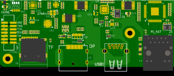
In recent years, additive PCB manufacturing has emerged as a game-changing approach in the field of electronics. This technique allows you to create circuit boards by adding layers of material rather than subtractively removing them from a larger piece. This method not only enhances the design flexibility but also addresses some of the common challenges faced by traditional PCB manufacturing companies. By leveraging processes like 3D printing and inkjet technology, you can significantly reduce the PCB manufacturing cost, making it a viable option for small to medium-scale PCB manufacturing business ventures.
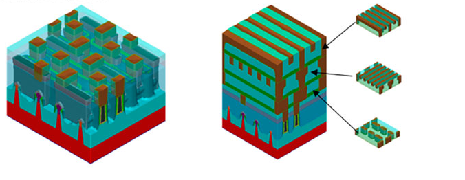
One notable advantage of additive techniques is their ability to minimize material waste. Unlike subtractive methods, which often lead to significant leftover materials, additive processes allow you to utilize precisely what you need for each project. This efficiency can be quantified in tables comparing traditional vs. additive methods, showcasing how additive PCB techniques lead to less waste and more sustainable practices.
“The future of PCB design is not just about faster production but also about smarter production.”
By adopting these innovative technologies, you are positioned not only to enhance your product offerings but also to be at the forefront of new developments in electronic design. Embracing additive PCB manufacturing could define a new era in your approach to circuit board fabrication, presenting opportunities for rapid prototyping and helping you stay competitive in an evolving market. If you’re looking to dive deeper into these advancements, exploring resources from Andwin PCB can provide valuable insights into the nuances of this innovative approach.
Benefits of Additive PCB Processes
The benefits of additive PCB processes in the realm of PCB manufacturing are significant and transformative. By adopting these advanced techniques, you can experience a remarkable reduction in both material waste and manufacturing costs. Traditional methods typically involve subtractive techniques that often generate excess waste, while additive PCB processes build layers directly, offering a more efficient alternative. This approach enables you to create complex designs with precision that is hard to achieve through conventional methods.
Moreover, as you collaborate with various PCB manufacturing companies, you will find that the ability to produce prototypes rapidly enhances your design development cycle. The benefits extend beyond mere cost savings; they include improved production efficiency and fast iterations that support innovative designs. In the competitive landscape of the PCB manufacturing business, utilizing additive techniques can position your company at the forefront, minimizing lead times and enabling quicker responses to market demands. This not only bolsters your credibility within the industry but also enhances overall customer satisfaction by meeting varying design needs effectively and efficiently.
In summary, embracing additive processes in your PCB manufacturing practices will not only streamline production but also address the growing need for customized electronic solutions with lower environmental impact, paving a sustainable path for future growth in this dynamic field.
Cutting-Edge Technologies in Additive PCB Fabrication
In recent years, additive PCB manufacturing has emerged as a revolutionary process that offers unprecedented opportunities for innovation in the electronics industry. With advancements in 3D printing, laser sintering, and other technologies, you can now achieve intricate designs that were once too costly or impractical via traditional methods. These cutting-edge solutions not only enhance the versatility of your designs but also significantly reduce pcb manufacturing cost, making it easier for businesses—especially pcb manufacturing companies—to engage in agile development cycles. By utilizing these modern techniques, your pcb manufacturing business can minimize material waste, ensuring a more sustainable approach to production while maintaining high-quality standards. As you delve into these technologies, you’ll discover how they transform your production methodologies and offer faster turnaround times, which is essential in today’s fast-paced market. The integration of such innovations allows for a seamless adaptation to complex electronic requirements, giving you a competitive edge in the dynamic landscape of electronics fabrication.
Efficiency and Material Waste Reduction in Additive Methods
In the realm of additive PCB manufacturing, efficiency and material waste reduction are paramount. By employing advanced techniques, you can achieve significant reductions in pcb manufacturing cost, ensuring that resources are utilized optimally. Traditional pcb manufacturing processes often involve excess material, leading to increased waste and escalating costs. However, with additive methods, each layer is precisely applied, ensuring that only the necessary materials are used for your designs. This not only enhances productivity but also minimizes the environmental impact associated with excess waste.
Moreover, leading pcb manufacturing companies are shifting towards additive processes that offer on-demand production capabilities. This innovation not only accelerates the design-to-production timeline but also allows for customization without the financial burden typically associated with large production runs. By streamlining these processes, you can enhance your pcb manufacturing business‘s agility in responding to market demands. Embracing these techniques positions you favorably within a competitive landscape while emphasizing sustainability—an important consideration for modern consumers and industries alike. Ultimately, integrating additive PCB methods into your operations helps to foster a culture of efficiency and responsibility, aligning with both economic and ecological goals.
Rapid Prototyping: Transforming Electronic Design Development
In today’s fast-paced technology landscape, rapid prototyping has emerged as a revolutionary technique in pcb manufacturing that significantly enhances your electronic design development process. Traditionally, the process of creating prototypes was time-consuming and often fraught with challenges related to costs and material waste. However, with the advent of innovative additive PCB manufacturing techniques, you now have the ability to quickly iterate designs and test functionalities at a fraction of the traditional pcb manufacturing cost. This approach allows you to create complex circuitry more efficiently and pinpoint potential flaws much earlier in the design cycle.
One of the primary advantages that pcb manufacturing companies enjoy through rapid prototyping is the ability to produce small batch runs without excessive overhead. By utilizing techniques like 3D printing and laser etching, these companies can adjust their designs on-the-fly, opening the door to creative exploration that was previously limited by extensive production timelines. As your project requirements evolve, being able to make swift modifications not only keeps costs down but also accelerates time-to-market for your innovations.
Moreover, rapid prototyping supports a deeper understanding of product functionality before full-scale production begins, enabling you to make informed decisions regarding your pcb manufacturing business strategies. As you integrate these advanced technologies into your workflow, you’ll discover that rapid prototyping is not just a method but a transformative approach that empowers you to achieve higher quality results with minimal waste. This is particularly essential in an era where sustainability is becoming increasingly prioritized in manufacturing practices. With these advancements at your disposal, you are well-positioned to push the boundaries of electronic design possibilities.
Future Trends in Additive PCB Manufacturing
As you navigate the world of additive PCB manufacturing, it’s essential to recognize the emerging trends shaping this field. The shift towards more flexible and efficient production methods reflects not only advancements in technology but also the evolving needs of PCB manufacturing companies. In the coming years, you can expect to see an increased focus on automation and smart manufacturing processes. These innovations aim to optimize PCB manufacturing cost and improve overall efficiency. Additionally, sustainability will play a crucial role, as manufacturers strive to minimize material waste while maintaining high standards in product quality.
Moreover, advancements in materials science will lead to the development of new substrates that offer enhanced performance characteristics for complex electronic designs. This shift will ensure that your PCB manufacturing business can keep up with the rising demand for high-frequency applications and compact circuit designs. The integration of artificial intelligence and machine learning into production systems will also significantly influence quality control, allowing for more reliable outputs with reduced human error and increased customization options.
Collectively, these trends illustrate a promising future for additive PCB techniques, where innovation meets sustainability, making it an exciting time for stakeholders within this dynamic industry.
Case Studies: Success Stories in Additive PCB Techniques
In the realm of pcb manufacturing, several companies have showcased remarkable success through innovative additive PCB techniques. One standout example is a small startup that dramatically reduced its pcb manufacturing cost while enhancing the quality of its products. By leveraging additive methods, this company streamlined its production process, allowed for intricate designs, and minimized material waste. They were able to produce complex circuit boards with unmatched precision in less time, which not only improved their turnaround times but also increased customer satisfaction. Another success story involves a well-established enterprise that integrated additive techniques into their existing pcb manufacturing business model. The transition empowered them to pivot towards more sustainable practices and reduced their dependency on traditional materials, positioning them as a leader among pcb manufacturing companies focused on environmental responsibility. These case studies illustrate how embracing advancements in additive PCB technologies can transform operations and create significant competitive advantages in the dynamic landscape of electronic design development.
Conclusion
In the rapidly evolving landscape of pcb manufacturing, the innovative approaches discussed throughout this article emphasize the significant advantages of additive PCB techniques. By adopting these methods, you can benefit from enhanced efficiency and a marked reduction in material waste, which are crucial for today’s competitive market. The ability to swiftly produce prototypes not only accelerates your design process but also allows you to tackle complex electronic designs with newfound agility. As you consider partnering with reputable pcb manufacturing companies, understanding the implications of pcb manufacturing costs on your business strategy is essential. You’ll find that investing in modern pcb manufacturing technologies can lead to a more sustainable, cost-effective, and efficient production process. The future trends highlighted indicate that as these technologies mature, they will play an integral role in shaping the landscape of the pcb manufacturing business, providing you with opportunities to innovate and stay ahead in your field.
FAQs
What is additive PCB manufacturing?
Additive PCB manufacturing refers to a process where layers of materials are added to create circuit boards, rather than removing material from a larger piece. This innovative approach can lead to reduced pcb manufacturing costs and enhanced design flexibility.
What are the benefits of using additive PCB processes?
Utilizing additive methods in pcb manufacturing allows for higher efficiency, decreased material waste, and the ability to create complex geometries that traditional methods struggle with. These benefits can be particularly advantageous for pcb manufacturing companies, as they strive for competitive edge in the market.
How does rapid prototyping fit into additive PCB manufacturing?
Rapid prototyping enables you to quickly iterate and test designs. This is crucial for businesses looking to innovate in their pcb manufacturing business, as it streamlines the development process and significantly reduces time-to-market.
What should I consider when choosing a PCB manufacturer?
When selecting among various pcb manufacturing companies, consider factors such as technology capabilities, cost efficiency, delivery timelines, and expertise in additive processes. This can influence your overall pcb manufacturing cost and the success of your projects.
For more in-depth information on these topics and best practices in PCB processes, please visit our resource on PCB Manufacturing.