Innovative Approaches to Design Fabrication and Assembly of PCBs

Key Takeaways
In the rapidly evolving field of printed circuit boards (PCBs), staying updated with current innovations is crucial for manufacturers and designers alike. The integration of advanced technologies has led to significant improvements in pcb assembly and overall production efficiency. Key advancements include the utilization of automated processes that minimize human error and increase production speed. Furthermore, pcba practices now emphasize precision in assembly, which is essential to meet industry standards and client specifications.
Recent trends showcase a shift towards using eco-friendly materials and implementing sustainable practices that not only enhance performance but also address environmental concerns. Cost reduction has become a pivotal factor in PCB manufacturing; innovative techniques such as using modular designs can significantly lower material waste and streamline production cycles.
Table 1 below illustrates the contrast between traditional manufacturing methods and modern practices, showcasing how contemporary approaches lead to enhanced quality and performance in pcb assembly:
| Aspect | Traditional Methods | Innovative Approaches |
|---|---|---|
| Production Speed | Slower due to manual processes | Faster with automation |
| Error Rate | Higher due to human involvement | Significantly lower |
| Material Waste | More wasteful | Reduced through precision design |
| Cost Efficiency | Higher operational costs | Lower costs with sustainable materials |
Adoption of these innovative strategies not only positions companies for better competitiveness but also enhances the functionality and durability of the final products, affirming the continuous evolution in the field of PCB design, fabrication, and assembly.
Introduction to PCB Technology and Its Importance
The significance of printed circuit boards (PCBs) in modern electronics cannot be overstated. As a foundational component, PCBs serve as the backbone that supports and interconnects various electronic parts. The evolution of PCB technology has been pivotal in the advancement of countless applications, ranging from consumer electronics to complex industrial machinery. With increasing demands for miniaturization and enhanced functionality, innovative strategies are essential for staying competitive.
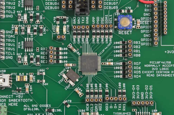
PCB assembly (PCBA) involves multiple stages that demand precision, effectiveness, and a deep understanding of both design and fabrication processes. Today’s designers employ cutting-edge software tools to create intricate layouts that optimize space and performance while ensuring manufacturability. Moreover, advancements in fabrication methods have significantly improved the precision and speed at which PCBs can be produced, leading to faster turnaround times and better quality products.
“Adopting a holistic approach to PCB design not only streamlines manufacturing but also elevates performance standards across the board.”
Focusing on efficiency in PCB assembly can drastically reduce costs associated with both materials and labor while improving the overall consistency of end products. As industries evolve, it becomes crucial to leverage such innovative practices in PCB manufacturing processes to meet consumer demands effectively. Thus, understanding the importance of PCB technology is fundamental for any stakeholder in the electronics industry who seeks sustainability and growth in an increasingly competitive marketplace.
Current Trends in PCB Design: Techniques and Tools
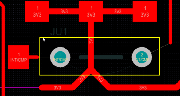
In the rapidly evolving field of printed circuit boards (PCBs), advancements in design methodologies and tools have become crucial for manufacturers seeking a competitive edge. One influential trend is the integration of computer-aided design (CAD) software that allows for greater precision during the design phase, which is essential for producing more complex circuitry. These tools facilitate rapid prototyping and testing, significantly decreasing development times. Additionally, simulation software is increasingly utilized to predict performance issues before physical prototypes are created, thus reducing waste and optimizing the functionality of pcb assembly processes.
Moreover, the shift towards lightweight and flexible materials has encouraged designers to rethink traditional methods; by employing materials like polyimide or flexible substrates, manufacturers can enhance the durability and versatility of PCBs. This transition is particularly beneficial in industries such as consumer electronics and medical devices where miniaturization is essential.
Another significant trend involves the enhancement of collaborative platforms, where designers can work in real-time with engineers to ensure that the design aligns closely with the manufacturing capabilities of pcba processes. This not only streamlines workflow but also fosters innovation through diverse input. By leveraging these modern tools and techniques, organizations are able to not only enhance efficiency but also maintain high standards in quality control throughout both fabrication and assembly, paving the way for future innovations in PCB technology.
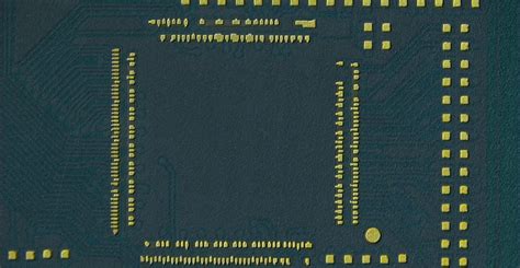
Advanced Fabrication Methods: Enhancing Precision and Speed
In the ever-evolving realm of printed circuit boards (PCBs), advanced fabrication methods have become pivotal in enhancing both precision and speed. As the demand for more intricate designs increases, manufacturers are adopting innovative techniques that leverage cutting-edge technology. One such approach is the implementation of laser machining, which allows for highly accurate cutting and engraving of PCB materials. This method not only enhances the quality of the final product but also accelerates production times by minimizing material waste. Furthermore, advancements in additive manufacturing have introduced new possibilities for creating complex geometries that were previously unattainable with traditional processes. These methods not only improve design flexibility but also contribute to a reduction in assembly errors during the pcb assembly phase, ultimately leading to higher performance in the final product.
Additionally, techniques like multi-layer stacking have gained traction, enabling engineers to optimize space within a circuit while enhancing signal integrity. This process streamlines the transition from design to fabrication, contributing significantly to efficiency gains in PCB production lines. When combined with automated optical inspection (AOI) systems during pcba, these fabrication innovations ensure that quality control is maintained at every stage, leading to a reduction in defect rates and improved reliability. Overall, these advanced fabrication methods signify a substantial leap forward in PCB technology, reinforcing their critical role in various high-tech applications across industries today.
Effective Assembly Strategies for High-Quality PCBs
The process of pcb assembly or PCBA is critical in ensuring the reliability and performance of electronic devices. Effective assembly strategies focus on optimizing the integration of electronic components onto printed circuit boards to achieve a high-quality end product. One notable approach is the use of automated pick-and-place machines, which enhance precision and speed during component placement, thereby minimizing human error and variability. Additionally, manufacturers are investing in advanced soldering technologies, such as selective soldering and laser soldering, which provide better results than traditional wave soldering methods. Employing these methods can improve thermal management and reduce the risk of component damage.
To further enhance quality, regular inspections using automated optical inspection (AOI) systems are essential for identifying defects early in the process. These systems can detect misplaced components, insufficient solder joints, or other issues that may arise during pcb assembly. Implementing a robust quality management system that includes thorough testing protocols ensures that each assembled board meets stringent performance standards before leaving the production facility.
Considering material choices is also paramount; using high-quality substrates and components can lead to improved durability and performance in the final product. By combining these advanced technologies with rigorous quality assurance measures, manufacturers can lower defect rates and boost overall efficiency in their PCB assembly processes, ultimately driving down costs while delivering high-quality printed circuit boards to market.
Cost Reduction Techniques in PCB Manufacturing
In an increasingly competitive landscape, achieving cost reduction in PCB manufacturing is crucial for sustaining market viability. One prominent strategy involves the optimization of the printed circuit board assembly (PCBA) processes. By employing techniques such as selective soldering, manufacturers can minimize waste and enhance efficiency. Furthermore, leveraging advanced software tools during the design phase can lead to fewer iterations and a more streamlined production line, ultimately resulting in lower costs. Additionally, implementing modular design principles allows for easier reconfiguration and reuse of components, which can significantly cut down on system redesign expenses. Manufacturers are also adopting automated testing methodologies to ensure quality assurance while reducing labor costs. These innovations not only drive the cost-effective manufacturing of PCBs but also contribute to improved product reliability and performance, marking a significant shift toward more efficient production practices in the electronics industry.
Sustainable Practices in Design and Fabrication of PCBs
The increasing emphasis on sustainability in printed circuit board (PCB) design and fabrication has led to innovative practices that not only benefit the environment but also enhance operational efficiency. One of the primary strategies is the use of eco-friendly materials that reduce the carbon footprint during production. For instance, manufacturers are now employing lead-free solder and recyclable substrates which are less harmful to the environment compared to traditional materials. Moreover, optimization of the pcb assembly process plays a vital role in sustainability; by improving layouts and component placement, companies can significantly minimize waste. In addition to material selection and process optimization, energy efficiency has become a focal point. Many leading firms are adopting renewable energy sources in their manufacturing facilities while implementing techniques such as automated inventory systems to better manage resources. Such strategies not only reduce costs but also align with global trends toward greener manufacturing practices. Furthermore, emphasizing pcba testing methods that identify defects early in the assembly process can help in reducing material waste and rework, thus promoting a more sustainable approach to PCB production. Ultimately, integrating sustainable practices into PCB design and fabrication is crucial for fostering an eco-conscious industry while simultaneously enhancing overall efficiency and product quality.
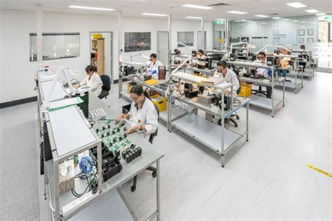
The Role of Automation in PCB Assembly Processes
The integration of automation in PCB assembly processes has significantly transformed the way printed circuit boards are manufactured and assembled. By incorporating advanced robotics and sophisticated software solutions, manufacturers can achieve a level of precision and efficiency that manual assembly techniques simply cannot match. Automated systems streamline the PCBA process, minimizing human error while enhancing consistency and speed in production. They are capable of quickly adapting to various design specifications, allowing for rapid prototyping and faster turnaround times for customers. Additionally, automated inspection systems ensure that each component is placed accurately and that the soldering meets stringent quality standards. The result is a marked improvement in the overall performance of the assembled PCBs, leading to more reliable electronic devices. As the demand for smaller, more complex assemblies grows, automation will continue to play a critical role in optimizing PCB assembly, reducing costs, and keeping pace with industry advancements. Ultimately, the shift toward automation not only benefits manufacturers but also enhances product quality for end-users by ensuring that every board meets the required specifications effectively.
Future Directions: Innovations Shaping the Future of PCBs
As technology continues to advance, the field of printed circuit boards (PCBs) is poised to undergo transformative changes. One of the most promising future directions involves the integration of smart technologies into PCB assembly processes, which enables real-time monitoring and adjustments during manufacturing. This not only enhances quality but also reduces waste by allowing for immediate corrections when discrepancies arise. Furthermore, advancements in materials science are leading to the development of innovative substrates and conductive materials that can improve the thermal management and electrical performance of PCBA. The push towards miniaturization has also driven techniques such as 3D printing and microfabrication methods that can produce smaller and more complex designs without compromising functionality. In addition, as sustainability becomes increasingly important, focusing on eco-friendly materials and recycling measures is essential for the future landscape of PCB manufacturing. The continued exploration of automation in PCB assembly, coupled with intelligent algorithms for design efficiency, promises to streamline operations further while minimizing labor costs. Overall, embracing these innovations will undoubtedly play a crucial role in shaping the efficiency and effectiveness of PCB design, fabrication, and assembly processes in the years to come.
Conclusion
In conclusion, the landscape of printed circuit boards (PCBs) and their assembly has evolved significantly, driven by the integration of innovative approaches throughout the design and fabrication stages. As highlighted in this article, a focus on advanced techniques not only enhances precision and efficiency but also addresses the pressing need for cost-effective solutions in PCB assembly. Furthermore, embracing sustainable practices ensures that industries can meet both economic and environmental responsibilities while delivering high-quality PCBA. The advancing role of automation continues to streamline the assembly processes, further improving reliability and performance. As we look to the future, it is evident that ongoing innovations will shape the development of PCBs, fostering an environment ripe for growth and transformation in this critical sector. Thus, staying abreast of these trends is essential for professionals in electronics manufacturing who aim to maintain a competitive edge in an ever-evolving market.
FAQs
What is PCB assembly?
PCB assembly, often abbreviated as PCBA, is the process of soldering electronic components onto a printed circuit board to create a functional device. This process includes various steps such as component placement, soldering, and inspection.
What are the major steps involved in PCBA?
The major steps in pcb assembly involve preparation of the PCB, placement of components, soldering (which may include wave soldering or surface mount technology), inspection, and testing to ensure quality and functionality.
How can I improve the quality of my PCB assembly?
Improving quality can be achieved through careful component selection, employing automated assembly techniques, implementing stringent quality control measures during each phase of pcba, and using high-quality materials in the initial design and fabrication stage.
What technologies are being used to enhance PCB assembly efficiency?
Technologies such as automated robotics for component placement, advanced software for design verification, and real-time monitoring systems are increasingly becoming essential for enhancing efficiency in pcb assembly.
How do I choose a reliable PCB assembly service provider?
When choosing a PCB assembly service provider, consider their experience in specific industries, their certifications (such as ISO standards), customer reviews, range of services offered (including design and testing), and their ability to handle various production volumes.