Innovative Methods in Copper Clad Board Manufacturing

Key Takeaways
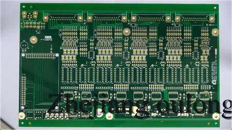
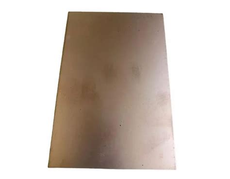
Modern copper clad board manufacturing integrates PCB assembly innovations with precision engineering to meet evolving industry demands. Key advancements include laser-direct structuring for circuit patterning and low-pressure lamination techniques that enhance layer adhesion while minimizing voids. Manufacturers now prioritize PCBA-compatible designs, ensuring seamless integration with automated assembly lines.
"Optimizing thermal conductivity in base materials reduces heat-related failures by up to 40% in high-frequency applications." – Industry White Paper
A comparative analysis reveals critical improvements:
| Parameter | Traditional Method | Advanced Method |
|---|---|---|
| Etching Precision | ±25 µm | ±8 µm |
| Thermal Resistance | 1.2°C/W | 0.6°C/W |
| Production Waste | 18% | 6% |
For PCB assembly workflows, manufacturers now deploy modified semi-additive processes (mSAP) to achieve finer trace widths below 15µm. Environmentally conscious approaches, such as halogen-free prepregs and lead-free surface finishes, align with global regulatory standards. When selecting materials for PCBA integration, consider:
- Glass transition temperature (Tg) stability above 180°C
- Dielectric constant consistency across frequency ranges
- Compatibility with reflow soldering profiles
These developments collectively reduce time-to-market by 22% while maintaining <0.5% defect rates in mass production.

Advanced Lamination Methods Unveiled
Modern copper clad board manufacturers are redefining lamination techniques to meet the escalating demands of PCB assembly and PCBA applications. By integrating multi-layer stacking with low-loss prepreg materials, these methods enhance signal integrity while minimizing dielectric losses. Innovations like automated optical alignment systems ensure micron-level precision in layer registration, critical for high-density interconnects in advanced PCBA designs.
The adoption of variable-pressure thermal pressing allows tailored curing profiles, reducing residual stress in laminated boards. This proves vital for applications requiring thermal cycling resilience, such as automotive electronics or aerospace PCB assembly. Additionally, manufacturers now utilize hybrid bonding technologies that combine thermosetting and thermoplastic adhesives, optimizing both mechanical stability and rework flexibility during PCBA repairs.
Transitioning toward sustainable practices, some facilities employ solvent-free prepreg systems that eliminate volatile organic compounds without compromising bond strength. These advancements not only align with eco-friendly initiatives but also improve production efficiency—a crucial factor as PCB assembly timelines shrink across industries. Such innovations lay the groundwork for exploring subsequent precision etching processes, ensuring seamless integration across the manufacturing chain.

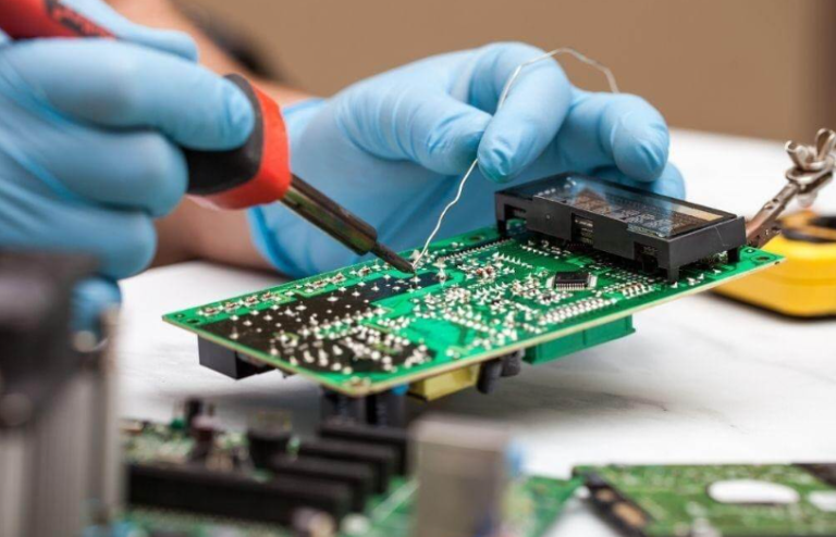
Precision Etching in PCB Production
Modern PCB assembly relies heavily on precision etching to achieve the microscopic circuitry required for high-performance electronics. This process begins with photolithography, where a photoresist layer is applied to the copper clad board and exposed to UV light through a patterned mask. The unexposed areas are then dissolved, leaving behind a precise template for etching. Advanced chemical etching solutions selectively remove unprotected copper, creating circuit traces as narrow as 15 microns—critical for compact PCBA designs.
Manufacturers now employ laser direct imaging (LDI) to enhance accuracy, eliminating traditional film-based masking and reducing alignment errors by up to 40%. Post-etching, automated optical inspection (AOI) systems verify trace integrity, ensuring compliance with stringent signal integrity standards. This level of precision directly impacts thermal performance, as evenly distributed copper layers minimize hotspots in high-frequency applications.
To balance efficiency and sustainability, closed-loop etching systems recover and reuse copper ions, aligning with broader trends in eco-friendly PCB fabrication. Such innovations not only refine circuit quality but also streamline integration with downstream PCB assembly processes, reducing lead times for complex multilayer boards. As demand grows for miniaturized electronics, optimized etching techniques remain pivotal in maintaining the delicate equilibrium between performance, cost, and scalability.
Eco-Friendly Copper Clad Processes
The shift toward sustainable manufacturing has led copper clad board manufacturers to adopt eco-friendly processes that minimize environmental impact while maintaining performance standards. Innovations include the use of low-VOC (volatile organic compound) laminates and water-based etching solutions, which reduce hazardous emissions during PCB assembly. Advanced recycling systems now recover up to 95% of copper waste from production lines, significantly lowering resource consumption. Additionally, manufacturers are integrating halogen-free flame retardants into substrates, aligning with global regulations like RoHS and REACH.
A critical advancement lies in energy-efficient lamination techniques, which cut power usage by 20–30% without compromising bond strength or thermal stability. These methods ensure compatibility with PCBA workflows, where heat dissipation and material durability are paramount. Some facilities also employ closed-loop water systems to treat and reuse etching byproducts, reducing freshwater dependency. By prioritizing circular economy principles, producers not only meet sustainability targets but also enhance cost predictability for high-volume orders. This balance of ecological responsibility and technical rigor positions eco-conscious copper clad boards as a cornerstone of modern electronics manufacturing.
Optimizing PCB Thermal Performance
Effective thermal management remains critical for modern PCB assembly processes, particularly as component density increases in advanced pcba designs. Manufacturers employ thermal conductivity mapping to identify hotspots, often integrating metal-core substrates or ceramic-filled laminates to enhance heat dissipation. Recent innovations include laser-drilled microvias that create optimized thermal pathways while maintaining circuit integrity—a technique particularly valuable in high-density interconnect applications.
For high-power PCB assemblies, engineers now prioritize coefficient of thermal expansion (CTE) matching between copper layers and dielectric materials, reducing mechanical stress during thermal cycling. Advanced thermally conductive adhesives further improve heat transfer in multilayer configurations. Real-time thermal simulation tools enable precise modeling of heat distribution patterns, allowing adjustments before pcba production begins—a strategy that reduces prototyping costs by up to 22%.
The shift toward lead-free solder alloys in PCB assembly introduces new thermal challenges, necessitating tighter control over reflow oven profiles. Some manufacturers now implement phase-change materials in critical areas to absorb transient thermal loads, achieving 15-30% improvements in thermal buffering capacity compared to conventional designs.

Cost-Efficient PCB Production Methods
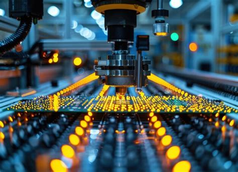
Modern manufacturers achieve cost efficiency in PCB assembly through strategic integration of automation and material optimization. Automated pick-and-place systems reduce labor costs while improving accuracy in component placement, particularly for high-volume PCBA orders. Advanced design-for-manufacturing (DFM) software minimizes material waste by optimizing circuit layouts and panel utilization, directly lowering raw copper clad laminate consumption.
Adoption of standardized processes, such as unified solder mask applications and controlled impedance testing protocols, reduces rework rates by up to 30%. Manufacturers further cut costs through bulk procurement of high-performance substrates and energy-efficient curing systems for solder masks. For specialized applications like LED lighting, some producers leverage aluminum-core boards to eliminate separate heat sinks, streamlining both production steps and thermal management costs.
Lean inventory models enabled by real-time PCBA demand forecasting ensure just-in-time material deliveries, avoiding overstocking of copper foils or prepreg materials. Hybrid manufacturing lines that switch between rigid and flexible board production further maximize equipment ROI. These methods collectively enable manufacturers to deliver competitively priced copper clad boards without compromising on the electrical reliability required for advanced IoT and automotive applications.
Next-Gen Circuit Board Materials
The evolution of PCB assembly technologies has driven significant advancements in substrate materials, particularly for high-performance applications. Modern copper-clad laminates now incorporate ceramic-filled polymers and low-loss resins, enabling superior signal integrity in high-frequency PCBA designs. Manufacturers are prioritizing materials with enhanced thermal conductivity, such as metal-core substrates, to address heat dissipation challenges in compact electronics.
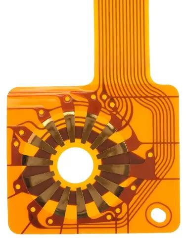
A notable innovation lies in flex-rigid hybrid boards, which combine polyimide films with reinforced epoxy layers to balance durability and flexibility. These materials reduce failure rates in PCB assembly by withstanding mechanical stress during component mounting. Additionally, graphene-infused copper foils are gaining traction for their ability to minimize signal loss while maintaining cost-efficiency—a critical factor for high-volume PCBA production.
Transitioning toward sustainable solutions, manufacturers are adopting halogen-free flame retardants and recyclable thermoplastics without compromising electrical performance. This shift aligns with global regulations while supporting faster prototyping cycles—a key advantage for industries requiring rapid iterations. As 5G and IoT applications expand, these next-gen materials are redefining reliability benchmarks across both consumer and industrial electronics sectors.
Innovative PCB Bonding Techniques
Modern PCB assembly relies on advanced bonding technologies to ensure structural integrity and electrical reliability in complex circuits. Thermal compression bonding has emerged as a key method, enabling precise alignment of multilayer boards while maintaining signal integrity at high frequencies. Manufacturers are increasingly adopting laser-assisted bonding systems, which reduce thermal stress on sensitive components during PCBA processes. These systems achieve micron-level accuracy, critical for high-density interconnect (HDI) designs.
A notable innovation involves anisotropic conductive films (ACFs), which create z-axis conductivity without short-circuiting adjacent traces. This technique is particularly valuable for bonding flexible circuits to rigid substrates, a common requirement in wearable electronics and IoT devices. For eco-conscious production, UV-curing adhesives are gaining traction, offering faster curing times and reduced energy consumption compared to traditional thermal methods.
To enhance durability in harsh environments, hybrid bonding approaches combine mechanical fasteners with conductive epoxies. Such methods improve vibration resistance in automotive or aerospace applications while maintaining electrical continuity. Leading manufacturers now integrate real-time monitoring systems during bonding phases, using sensors to track adhesion strength and cure rates for quality assurance. By optimizing these techniques, PCBA workflows achieve higher yields and lower defect rates, directly impacting cost-efficiency in high-volume production.
Sustainable PCB Fabrication Practices
The electronics manufacturing sector is increasingly prioritizing eco-conscious approaches in PCB assembly workflows, driven by regulatory demands and corporate sustainability goals. Leading copper clad board manufacturers now integrate closed-loop systems to reclaim copper residues from etching processes, reducing raw material consumption by up to 40%. Advanced water-soluble photoresists and halogen-free laminates are replacing traditional solvents, minimizing volatile organic compound (VOC) emissions during PCBA production.
To enhance energy efficiency, factories deploy infrared preheating systems for lamination, cutting energy use by 25% compared to conventional methods. Innovations like laser-direct imaging (LDI) further streamline patterning accuracy while eliminating chemical developers, aligning with global circuit manufacturing standards. Recyclable solder masks and lead-free finishes are becoming standard, ensuring end-of-life PCB assemblies meet WEEE directive requirements.
Manufacturers also adopt digital twin technology to simulate material flows, optimizing scrap rates during PCBA panelization. Third-party certifications like IPC-1401 validate these sustainable practices, creating verifiable benchmarks for low-carbon circuit board production. By balancing ecological responsibility with technical precision, the industry is redefining how high-performance electronics achieve both durability and environmental compliance.

Conclusion
As the copper clad board manufacturing industry progresses, manufacturers are strategically integrating advanced methodologies with traditional practices to address evolving demands in electronics. The convergence of PCB assembly innovations and sustainable material science has redefined production benchmarks, particularly in achieving tighter tolerances during PCBA stages. By implementing laser-direct structuring and additive manufacturing techniques, producers now achieve unprecedented precision in multilayer board construction while reducing material waste.
A critical development lies in harmonizing thermal management solutions with eco-conscious substrate formulations, enabling copper clad board manufacturers to meet both high-frequency performance requirements and RoHS compliance standards. This dual focus ensures that PCB assembly workflows maintain cost efficiency without compromising signal integrity in final PCBA products. Forward-looking facilities are further adopting predictive maintenance algorithms and real-time quality analytics to preemptively address potential defects across etching and lamination phases.
The sector’s trajectory underscores a balanced approach where circuit miniaturization trends coexist with robust durability enhancements—a synergy made possible through continuous R&D investments in dielectric materials and conductive adhesives. As regulatory pressures and consumer expectations intensify, this equilibrium between technical innovation and environmental stewardship will remain pivotal for sustainable growth in board fabrication ecosystems.

FAQs
How do material choices affect copper clad board performance in high-frequency applications?
Manufacturers select specialized dielectric materials with controlled dielectric constants to minimize signal loss. Advanced PCB assembly processes often pair these with ultra-thin copper foils (≤12μm) to enhance impedance matching.
What innovations improve thermal management in modern PCBs?
Embedded thermal vias and ceramic-filled prepregs distribute heat efficiently, critical for PCBA reliability in power electronics. Some producers now integrate graphene-doped substrates, achieving 20% better thermal conductivity than traditional FR-4 materials.
Are eco-friendly manufacturing methods compromising durability?
Next-gen halogen-free laminates and water-based etchants meet IPC-4101E standards while maintaining 95%+ bond strength. Laser-direct imaging further reduces chemical waste without sacrificing precision etching accuracy.
How do cost-efficient strategies impact multilayer board production?
Panel utilization algorithms and standardized PCB assembly tooling cut material waste by 18–22%. Automated optical inspection (AOI) systems also minimize rework costs, particularly in high-volume PCBA orders.
Can recycled copper foils meet industrial performance requirements?
Electrorefined recycled copper now achieves ≥99.9% purity, matching virgin material in conductivity tests. Manufacturers combine these with low-loss resins to create sustainable 4–32 layer boards for consumer electronics.
Ready to Optimize Your PCB Project?
For tailored PCB assembly solutions integrating these innovations, please click here to consult our engineering team.