Innovative Techniques for High-Performance Circuit Board Assembly

Key Takeaways
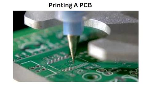
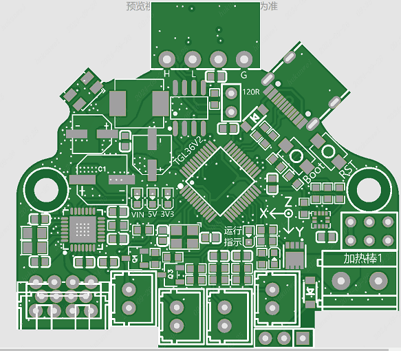
Modern PCB assembly processes leverage precision engineering to achieve micron-level accuracy in component placement, ensuring optimal electrical performance in compact designs. Automated soldering systems now integrate AI-driven vision inspection, reducing defect rates in PCBA by over 40% compared to manual methods. The adoption of low-loss dielectric materials and high-temperature substrates has enabled manufacturers to support 5G and IoT applications while maintaining thermal stability.
A critical advancement lies in laser-direct imaging (LDI) technology, which enhances trace definition for high-density interconnects (HDI) during PCB assembly. Combined with predictive maintenance algorithms, these innovations minimize downtime in production lines. Industry data shows that combining automated optical inspection (AOI) with machine learning reduces false defect calls by 62%, streamlining quality assurance in PCBA workflows.
These techniques collectively address the growing demand for reliability in aerospace, automotive, and medical devices, where even minor flaws in PCB assembly can lead to catastrophic failures. By balancing material science breakthroughs with intelligent automation, manufacturers achieve tighter tolerances while scaling production efficiently.

Precision Engineering in PCB Assembly
At the core of modern PCB assembly lies precision engineering, a discipline that ensures every micron-scale component aligns perfectly to meet rigorous performance standards. Advanced machinery, such as laser-guided pick-and-place systems and automated optical inspection (AOI) tools, now enable manufacturers to achieve tolerances as tight as ±25 micrometers. This level of accuracy is critical for high-density designs, where even minor misalignments in PCBA processes can lead to signal degradation or thermal inefficiencies.
The integration of surface-mount technology (SMT) has further refined precision in PCB assembly, allowing components as small as 01005 packages (0.4mm x 0.2mm) to be placed reliably. Real-time feedback systems monitor solder paste deposition and component orientation, reducing placement errors by over 60% compared to manual methods. Additionally, innovations in material handling—such as vacuum-controlled grippers and anti-static conveyors—minimize contamination risks during PCBA stages.
By harmonizing mechanical accuracy with intelligent process controls, precision engineering not only elevates board reliability but also lays the groundwork for scalable automation in subsequent manufacturing phases. These advancements ensure that today’s PCB assembly workflows meet the escalating demands of 5G, IoT, and AI-driven hardware ecosystems.
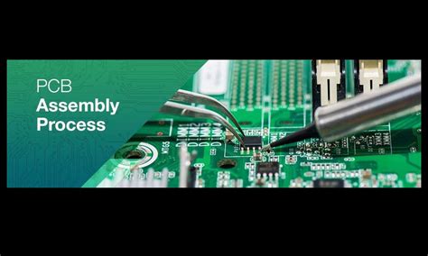
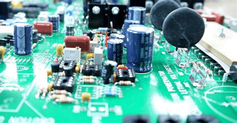
Automated Soldering Reduces PCB Defects
The adoption of automated soldering in PCB assembly has become a cornerstone for minimizing defects in modern electronics manufacturing. Unlike manual processes, which are prone to inconsistencies, robotic soldering systems leverage precision temperature control and vision-guided placement to ensure flawless solder joints. This shift is particularly impactful in PCBA workflows, where even minor errors can compromise circuit reliability.
Key technologies driving this transformation include:
| Technology | Defect Reduction Impact | Key Benefit |
|---|---|---|
| Robotic Soldering Arms | 40-60% | Eliminates human variability |
| Laser Soldering | 50-70% | Precision for micro-component joints |
| AOI (Automated Optical Inspection) | 30-50% | Real-time defect detection |
By integrating these systems, manufacturers achieve tighter tolerances in PCB assembly, reducing common issues like cold joints, bridging, and component misalignment. For instance, laser soldering enables sub-millimeter accuracy, critical for high-density PCBA designs. Additionally, closed-loop feedback mechanisms adjust parameters dynamically, ensuring consistent quality across production batches.
Another critical component is the use of lead-free solder alloys, which pair with automated systems to meet environmental regulations without sacrificing joint integrity. As a result, industries ranging from aerospace to consumer electronics report fewer field failures and lower rework costs, solidifying automated soldering as a non-negotiable standard in high-performance PCB assembly.

Material Innovations in PCB Manufacturing
Recent advancements in substrate materials are redefining quality standards for PCB assembly processes. Engineers now leverage high-frequency laminates and low-loss dielectrics to minimize signal interference in high-speed applications, particularly for PCBA designs requiring millimeter-wave functionality. The adoption of ceramic-filled polymers has improved thermal conductivity by up to 15%, enabling better heat dissipation in compact, power-dense layouts.
"Material science breakthroughs directly influence reliability," notes Dr. Elena Torres, a materials engineer at CircuitTech Labs. "New substrates reduce warping during reflow soldering, which is critical for maintaining structural integrity in multi-layer boards."
Halogen-free flame-retardant substrates are gaining traction, aligning with global sustainability mandates while reducing toxic byproducts in PCB assembly workflows. These materials also exhibit enhanced compatibility with automated soldering systems, lowering defect rates caused by thermal mismatches. Additionally, innovations like silver-nanoparticle conductive inks enable finer trace resolutions, supporting the trend toward miniaturized components in advanced PCBA applications.
To optimize performance, manufacturers are testing hybrid materials that combine rigid and flexible properties, allowing seamless integration of bendable circuits into traditional rigid-board architectures. This approach not only extends product lifespans but also simplifies PCB assembly for complex, mixed-form-factor designs.
High-Performance PCB Assembly Techniques
Modern PCB assembly processes rely on cutting-edge methodologies to meet the escalating demands for speed, reliability, and miniaturization. Central to these advancements is the integration of high-density interconnect (HDI) technology, which enables tighter component placement while maintaining signal integrity. By employing automated optical inspection (AOI) systems, manufacturers can detect micron-level defects in PCBA units, ensuring compliance with stringent quality standards.
Another critical innovation involves laser direct imaging (LDI), which enhances trace accuracy during solder mask application, minimizing impedance mismatches in high-frequency circuits. Additionally, advanced surface-mount technology (SMT) platforms now utilize precision nozzles and vision-guided robotics to place components at speeds exceeding 50,000 placements per hour. These systems are further enhanced by thermocompression bonding techniques, which create robust interconnects for fine-pitch BGAs and QFN packages.
To address thermal management challenges in high-performance applications, PCB assembly workflows increasingly incorporate metal-core substrates and embedded passive components. These material choices, combined with predictive analytics for reflow profiling, reduce thermal stress-induced failures by up to 32%. By leveraging these synergistic technologies, modern PCBA production achieves sub-10ppm defect rates while supporting operating frequencies beyond 100GHz. This evolution underscores the industry’s shift toward intelligent, data-driven manufacturing ecosystems.
Reducing Defects in PCB Production
Minimizing errors in PCB assembly remains a critical focus for manufacturers aiming to deliver reliable, high-performance electronics. Modern PCBA processes leverage real-time monitoring and machine learning algorithms to identify anomalies during production, enabling rapid corrections before defects propagate. For instance, automated optical inspection (AOI) systems scan solder joints and component placements at micron-level precision, flagging issues like misalignments or insufficient solder volume. Similarly, X-ray inspection is increasingly deployed for multilayer boards to detect hidden flaws such as voids in ball grid arrays (BGAs).
A key strategy involves optimizing design for manufacturability (DFM) principles, which align circuit layouts with production capabilities to prevent soldering failures or thermal stress. Advanced PCB assembly lines also integrate statistical process control (SPC) tools, analyzing data from each stage to refine parameters like reflow oven temperatures or stencil printing pressure. Additionally, the adoption of no-clean fluxes and moisture-resistant substrates reduces contamination risks, particularly in high-density PCBA applications. By combining these methodologies, manufacturers achieve defect rates below 50 parts per million (PPM), ensuring robust performance in demanding environments like automotive or aerospace systems.
To maintain consistency, rigorous supply chain audits ensure component authenticity, while humidity-controlled storage prevents oxidation of sensitive materials. This holistic approach underscores how innovation in PCB assembly not only elevates quality but also drives cost efficiencies across the product lifecycle.
Advanced Circuit Board Assembly Methods
Modern PCB assembly processes leverage cutting-edge technologies to address the demands of high-density, high-speed electronics. Central to these advancements is the integration of laser-assisted alignment systems, which enable micron-level positioning accuracy for surface-mount components. This precision minimizes parasitic capacitance and ensures optimal signal integrity in multi-layered PCBA designs. Automated optical inspection (AOI) systems now employ machine learning algorithms to detect soldering defects like voids or bridges with 99.7% accuracy, significantly reducing post-production rework.
A critical innovation lies in hybrid PCB assembly workflows, combining robotic pick-and-place machines with conductive adhesive dispensing for non-standard components. These systems achieve placement speeds exceeding 85,000 components per hour while maintaining ±15μm repeatability. For high-frequency applications, low-loss dielectric materials are paired with silver-filled epoxy to create stable interconnects in PCBA configurations. Thermal management has also evolved, with embedded copper pillars and direct-bonded copper substrates becoming standard for power electronics.
Transitioning toward these methods requires rigorous process validation, particularly when handling ultra-fine-pitch components below 0.3mm. Advanced flux chemistry formulations now enable void-free soldering under nitrogen atmospheres, critical for aerospace-grade assemblies. As the industry shifts to panel-level packaging, these techniques collectively enhance yield rates while supporting the miniaturization trends driving next-generation electronics.
Enhancing PCB Systems with Automation
Modern PCB assembly processes are increasingly reliant on automation to achieve the precision and consistency demanded by high-performance electronics. By integrating robotic systems into PCBA workflows, manufacturers can execute tasks such as component placement and solder paste application with micron-level accuracy, minimizing human error. Automated optical inspection (AOI) systems further enhance quality control by scanning boards for defects like misaligned components or solder bridging in real time, enabling immediate corrections.
Advanced programmable logic controllers (PLCs) synchronize assembly stages, from solder reflow profiling to final testing, ensuring seamless transitions between PCB assembly phases. This integration not only accelerates production cycles but also supports scalability for high-volume orders. Additionally, machine learning algorithms are now being deployed to analyze historical PCBA data, predicting potential failure points and optimizing process parameters dynamically.
Transitioning to automated systems reduces reliance on manual intervention, cutting defect rates by up to 60% in some cases. However, successful implementation requires balancing capital investment with long-term gains in yield and reliability—a critical consideration for manufacturers aiming to stay competitive in evolving markets.

Conclusion
The evolution of PCB assembly processes underscores the critical role of integrating precision engineering, automation, and material science to meet the demands of modern electronics. By leveraging advanced PCBA methodologies, manufacturers achieve unprecedented levels of reliability and performance in assembled circuit boards, while systematically reducing defects. Techniques such as automated optical inspection (AOI) and high-precision pick-and-place systems ensure consistency, particularly in complex, multi-layered designs. Furthermore, innovations like low-temperature soldering alloys and high-frequency substrate materials directly address thermal and signal integrity challenges.
As industries push toward miniaturization and higher power densities, the synergy between PCB assembly workflows and intelligent manufacturing ecosystems becomes indispensable. This convergence not only accelerates production timelines but also enhances scalability for high-mix, low-volume applications. Looking ahead, the adoption of AI-driven process optimization and sustainable material alternatives will likely define the next frontier in PCBA excellence, ensuring that cutting-edge electronics remain both efficient and environmentally conscious.
FAQs
How does automation improve quality in PCB assembly?
Automated systems in PCBA processes reduce human error by maintaining consistent soldering temperatures and component placement accuracy. This ensures repeatable precision, particularly for high-density boards requiring micron-level tolerances.
What role do material innovations play in modern PCB production?
Advanced substrates like high-frequency laminates and low-loss dielectrics minimize signal degradation in PCB assembly. These materials, combined with lead-free solder alloys, enhance thermal stability and compliance with environmental regulations.
Can automated optical inspection (AOI) eliminate all defects?
While AOI systems detect up to 98% of soldering flaws and misalignments in PCBA, complementary techniques like X-ray inspection are critical for verifying hidden connections in multilayer boards.
How do thermal management strategies affect high-performance PCB systems?
Integrating thermally conductive adhesives and copper-core substrates during PCB assembly dissipates heat more effectively, preventing component failure in power-intensive applications like 5G infrastructure.
Explore Professional PCB Assembly Solutions
For tailored PCB assembly services leveraging cutting-edge automation and material science, please click here to consult with industry experts.
Why is component sourcing crucial for reliable PCBA outcomes?
Collaborating with certified suppliers ensures access to counterfeit-free components and reduces lead times. Robust sourcing protocols directly impact yield rates in PCB assembly, especially for aerospace or medical-grade applications.