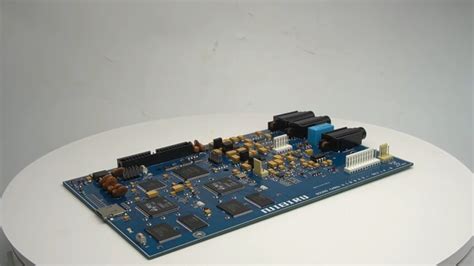
Introduction to Common PCB Inspection Technology and Equipment
No matter what type of printed circuit board needs to be built, or what type of equipment is used, the PCB must work properly. It is key to the performance of many products, and failure can have serious consequences.
Inspecting PCBs during the design, manufacturing, and assembly processes is essential to ensure that products meet quality standards and operate as expected. Today, PCBs are very complex. While this complexity provides room for many new features, it also brings a greater risk of failure. As PCBs have evolved, so have the inspection technology and the technology used to ensure their quality.
Choose the right inspection technology by PCB type, the current step in the production process, and the faults you want to test for. Developing a suitable inspection and test plan is essential to ensure a high-quality product.
Why do you need to inspect PCBs?
Inspection is a key step in all PCB production processes. It detects defects in PCBs so that they can be corrected and overall performance improved.
Inspecting PCBs can reveal any defects that may have occurred during the manufacturing or assembly process. It can also help reveal any design flaws that may exist. Inspecting PCBs after each stage of the process can detect defects before moving on to the next stage, avoiding wasting more time and money on defective products. It can also help find one-off defects that affect one or more PCBs. This process helps ensure consistent quality between the board and the final product.
Without a proper PCB inspection program, defective boards may be delivered to customers. If a customer receives a defective product, the manufacturer may lose money due to warranty payments or returns. Customers will also lose trust in the company, which can damage the company’s reputation. This situation can lead to missed opportunities if customers take their business elsewhere.
In the worst case, a defective PCB can cause injury or death if it is used in a product such as a medical device or automotive component. Such a problem can lead to serious reputational damage and expensive litigation.
Inspecting PCBs can also help improve the entire PCB production process. If a defect is frequently found, steps can be taken during the process to correct it.
Printed Circuit Board Assembly Inspection Methods
What is PCB Inspection? To ensure that PCBs will function as expected, manufacturers must verify that all components are assembled correctly. This is done through a range of techniques, from simple manual inspections to automated testing using advanced PCB inspection equipment.
Manual visual inspections are a good place to start. They may be all that is needed for relatively simple PCBs.
Manual Visual Inspection
The simplest form of PCB inspection is manual visual inspection (MVI). To perform this type of testing, workers view the board with the naked eye or under magnification. They will compare the board to the design documents to ensure that all specifications are met. They will also look for common defaults. The types of defects they look for depend on the type of board they are inspecting and the components on it.
It is useful to perform MVI after almost every step of the PCB production process, including assembly.
Inspectors examine almost every aspect of the board and look for a variety of common defects in each area. A typical visual PCB inspection checklist may include the following:
l Ensure the board thickness is correct and check for surface roughness and warpage.
l Check that the dimensions of the components meet specifications, paying special attention to those related to electrical connectors.
l Check the integrity and clarity of the conductive pattern and check for solder bridging, opens, burrs, and voids.
l Check the surface quality and then check for dents, dents, scratches, pinholes, and other defects on the printed traces and pads.
l Confirm that all vias are in the correct location. Ensure that no holes are missed or punched incorrectly, that the diameter matches the design specifications, and that there are no voids or nubs.
l Check the pad for firmness, roughness, and brightness, and check for raised defects.
l Evaluate coating quality. Check the color of the plating flux, and whether it is uniform, firm, and properly positioned.
MVI has several advantages over other types of inspection. It is low-cost due to its simplicity. No specialized equipment is required, except for possible magnification. These inspections can also be performed very quickly, and they are easy to add to the end of any process.
To perform this type of inspection, the only thing required is to find a professional staff member. If the necessary expertise is available, this technology can be helpful. However, it is crucial that the staff has access to the design specifications and knows which defects to watch out for.
This inspection method has limited capabilities. It cannot inspect components that are not within the worker’s line of sight. For example, hidden solder joints cannot be inspected with this method. The employee may also miss some defects, especially small ones. Inspecting complex boards with many small components using this method is particularly challenging.
Automated Optical Inspection
Visual inspection can also be performed using a PCB inspection machine. This method is called automated optical inspection (AOI).
AOI systems use multiple light sources and one or more still or video cameras to perform inspections. The light sources illuminate the PCB board from various angles. The cameras then take still images or videos of the board, compiling them to create a complete picture of the device. The system then compares the images it captures with information about the board’s appearance obtained from design specifications or approved complete units.
Both 2D and 3D AOI equipment are available. 2D AOI machines use colored lighting from multiple angles and side cameras to inspect components that are affected by their height. 3D AOI equipment is newer and can quickly and accurately measure component heights.
AOI can find many of the same defects as MVI, including nodules, scratches, opens, solder thinning, missing components, and more.
AOI is a mature, accurate technology that can detect many of the faults in PCBs. It is very useful at many stages of the PCB production process. It is also faster than MVI and eliminates the possibility of human error. Like MVI, it cannot be used to inspect components that are out of sight, such as connections hidden under ball grid arrays (BGAs) and other types of packaging. This may also not be effective for PCBs with a high concentration of components, as some of them may be hidden or obscured.
Automated Laser Test Measurement
Another method of PCB inspection is automated laser test (ALT) measurement. The dimensions of solder joints and solder deposits, as well as the reflectivity of various components, can be measured using ALT.
ALT systems use lasers to scan PCB components and take measurements. The system uses the position of the light as it reflects off the board’s components to determine their height. It also measures the intensity of the reflected beam to determine the reflectivity of the component. The system can then compare these measurements to design specifications or to a board that has been approved to accurately identify any defects.
Using an ALT system is ideal for determining the amount and location of solder paste deposits, and it provides information about the alignment, viscosity, cleanliness, and other properties of the solder paste print. The ALT method provides detailed information and can be measured very quickly. These types of measurements are generally accurate, but can be subject to interference or shielding.
X-ray Inspection
PCBs have become increasingly complex with the rise of surface mount technology. Today, circuit boards are denser, have smaller components, and include chip packages like BGAs and chip-scale packages (CSPs) through which hidden solder connections cannot be seen. These features create challenges for visual inspections like MVI and AOI.
To overcome these challenges, X-ray inspection equipment can be used. Materials absorb X-rays based on their atomic weight. Heavier elements absorb more, while lighter elements absorb less, which allows the materials to be differentiated. Solder is made of heavy elements like tin, silver, and lead, while most other components on a PCB are made of lighter elements like aluminum, copper, carbon, and silicon. As a result, solder is easily visible during X-ray inspection, while almost all other components, including substrates, leads, and silicon integrated circuits, are invisible.
Rather than being reflected like light, X-rays pass through an object, forming an image of the object. This process allows chip packages and other components to be inspected to see the solder connections underneath them. X-ray inspection also allows one to see inside solder joints to find bubbles that cannot be seen using AOI.
X-ray systems can also see the heels of solder joints, which would be obscured by the leads during AOI. Additionally, when using X-ray inspection, there are no shadows that can enter. Therefore, X-ray inspection works well for boards with dense components. X-ray inspection can be done manually using X-ray inspection equipment, or automated X-ray inspection (AXI) using an automated X-ray system.
X-ray inspection is ideal for more complex boards and has some features that other inspection methods don’t, such as the ability to see through chip packages. It also works well for inspecting densely packed PCBs and allows for a more detailed inspection of solder joints. The technology is a bit newer, more complex, and can be more expensive. Investing in X-ray inspection equipment is only necessary if you have a lot of densely packed boards with BGAs, CSPs, and other such packages.


