Introduction to Flex PCB Design Using KiCad
Flexible Printed Circuit Boards (Flex PCBs) have become increasingly popular in modern electronics due to their ability to bend, fold, and conform to unique shapes. This flexibility allows for innovative designs that are not possible with traditional rigid PCBs. KiCad, an open-source Electronic Design Automation (EDA) tool, has emerged as a powerful platform for designing Flex PCBs. This article will explore the fundamentals of Flex PCB design using KiCad, covering the key concepts, design considerations, and step-by-step guidance to help you create your own flexible circuits.
1. Understanding Flex PCBs
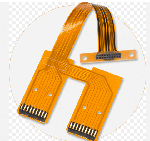
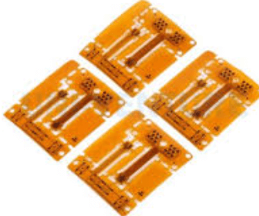
Flex PCBs are made from flexible substrate materials, such as polyimide, which allow the board to bend and twist without breaking. They are commonly used in applications where space and weight are critical, such as wearable devices, medical equipment, aerospace systems, and consumer electronics like smartphones and laptops.
Advantages of Flex PCBs:
- Space Efficiency: Flex PCBs can be folded or bent to fit into tight spaces.
- Weight Reduction: They are lighter than rigid PCBs, making them ideal for portable devices.
- Durability: Flex PCBs can withstand vibrations, shocks, and repeated bending.
- Simplified Assembly: They reduce the need for connectors and cables, simplifying the overall design.
Types of Flex PCBs:
- Single-Layer Flex PCBs: Consist of a single conductive layer on a flexible substrate.
- Double-Layer Flex PCBs: Have two conductive layers with an insulating layer in between.
- Multi-Layer Flex PCBs: Include multiple conductive layers, enabling complex designs.
- Rigid-Flex PCBs: Combine rigid and flexible sections, offering the benefits of both.
2. Introduction to KiCad
KiCad is a free, open-source EDA tool that provides a comprehensive suite of applications for PCB design. It includes tools for schematic capture, PCB layout, 3D visualization, and Gerber file generation. KiCad supports Flex PCB design, making it an excellent choice for hobbyists, engineers, and professionals.
Key Features of KiCad:
- Cross-Platform Compatibility: Works on Windows, macOS, and Linux.
- Open-Source: Free to use and modify, with a large community for support.
- Comprehensive Toolset: Includes schematic editor, PCB editor, 3D viewer, and more.
- Flex PCB Support: Allows for the creation of flexible and rigid-flex designs.
3. Designing Flex PCBs in KiCad
Designing Flex PCBs in KiCad involves several steps, from schematic creation to finalizing the layout. Below is a step-by-step guide to help you get started.
Step 1: Schematic Design
- Open KiCad and Create a New Project.
- Use the Schematic Editor (Eeschema) to Draw the Circuit:
- Add components and connect them using wires or labels.
- Assign footprints to each component.
- Run the Electrical Rules Check (ERC):
- Ensure there are no errors in the schematic.
Step 2: PCB Layout
- Open the PCB Editor (Pcbnew):
- Import the netlist from the schematic editor.
- Define the Board Outline:
- Use the “Edge.Cuts” layer to draw the shape of the Flex PCB.
- For Flex PCBs, consider the bending areas and ensure they are free of components.
- Place Components:
- Arrange components on the board, keeping in mind the flexibility requirements.
- Avoid placing components in areas that will bend or flex.
- Route Traces:
- Use the “Route Tracks” tool to connect components.
- For Flex PCBs, use curved traces instead of sharp angles to reduce stress on the copper.
- Add Flex-Specific Features:
- Use the “Zone” tool to create stiffeners (rigid sections) if needed.
- Add teardrops to improve mechanical strength at pad connections.
Step 3: Design Rule Check (DRC)
- Run the DRC:
- Check for errors such as short circuits, clearance violations, or missing connections.
- Adjust the Design:
- Fix any issues identified by the DRC.
Step 4: 3D Visualization
- Use the 3D Viewer:
- Visualize the Flex PCB in 3D to ensure it meets the design requirements.
- Check for component placement and bending areas.
Step 5: Generate Manufacturing Files
- Export Gerber Files:
- Generate Gerber files for each layer (e.g., copper, solder mask, silkscreen).
- Export Drill Files:
- Generate Excellon drill files for holes and vias.
- Provide Additional Instructions:
- Include notes for the manufacturer about the flexible areas, bend radius, and material specifications.
4. Design Considerations for Flex PC
Designing Flex PCBs requires careful consideration of several factors to ensure reliability and performance.
Bend Radius:
- The bend radius is the minimum radius at which the Flex PCB can be bent without damage.
- A smaller bend radius increases the risk of cracking or breaking.
- As a rule of thumb, the bend radius should be at least 6 times the thickness of the Flex PCB.
Material Selection:
- Polyimide is the most common substrate material due to its flexibility and thermal stability.
- Choose copper thickness based on current requirements and flexibility needs.
Trace Routing:
- Use curved traces instead of sharp angles to reduce stress on the copper.
- Avoid routing traces in bending areas if possible.
Stiffeners:
- Stiffeners are rigid materials (e.g., FR4) added to specific areas to provide support.
- They are often used in areas with connectors or heavy components.
Component Placement:
- Avoid placing components in bending areas.
- Use surface-mount devices (SMDs) instead of through-hole components for better flexibility.
Layer Stackup:
- For multi-layer Flex PCBs, ensure proper alignment of layers to prevent delamination.
- Use adhesive layers to bond the flexible and rigid sections in rigid-flex designs.
5. Challenges and Solutions in Flex PCB Design
Challenge 1: Mechanical Stress
- Flex PCBs are subject to mechanical stress during bending and flexing.
- Solution: Use curved traces, avoid sharp angles, and adhere to the recommended bend radius.
Challenge 2: Signal Integrity
- High-speed signals can be affected by the flexible nature of the PCB.
- Solution: Use controlled impedance routing and minimize the length of high-speed traces.
Challenge 3: Thermal Management
- Flex PCBs may have limited heat dissipation compared to rigid PCBs.
- Solution: Use thermal vias and ensure proper ventilation in the design.
6. Conclusion
Flex PCBs offer unparalleled design flexibility, making them ideal for modern electronics. KiCad, with its robust set of tools and open-source nature, provides an excellent platform for designing Flex PCBs. By following the steps outlined in this article and considering the key design factors, you can create reliable and efficient Flex PCBs for your projects. Whether you’re a hobbyist or a professional, KiCad empowers you to push the boundaries of innovation in electronics design.
This article provides a comprehensive overview of Flex PCB design using KiCad. With practice and attention to detail, you can master the art of creating flexible circuits and unlock new possibilities in your electronic designs.


