Introduction to Wet Film Process in PCB Manufacturing
Abstract
The wet film process is a critical step in the fabrication of printed circuit boards (PCBs), enabling the precise transfer of circuit patterns onto copper-clad laminates. This article provides a comprehensive overview of the wet film process, including its principles, key steps, advantages, disadvantages, and applications in modern PCB manufacturing. The discussion covers photoresist coating, exposure, development, etching, and stripping, along with comparisons to dry film alternatives. By understanding the wet film process, manufacturers can optimize production efficiency and improve PCB quality.
1. Introduction
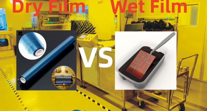
Printed circuit boards (PCBs) are essential components in electronic devices, providing mechanical support and electrical connections between components. The wet film process is a photolithographic technique used to define conductive traces on PCBs by selectively removing unwanted copper. Unlike dry film photoresist, which comes in pre-laminated sheets, wet film involves liquid photoresist application, offering unique benefits in fine-line PCB production.
2. Overview of Wet Film Photoresist
Wet film photoresist is a light-sensitive liquid polymer applied to copper-clad substrates. Once coated, exposed to UV light through a photomask, and developed, it forms a protective layer that resists chemical etching. The key characteristics of wet film photoresist include:
- High resolution for fine-line circuitry
- Excellent adhesion to copper surfaces
- Chemical resistance to acidic or alkaline etchants
- Compatibility with both subtractive and additive PCB processes
3. Key Steps in the Wet Film Process
3.1 Surface Preparation
Before applying wet film, the copper surface must be cleaned to remove oxides, dust, and contaminants. Common cleaning methods include:
- Mechanical scrubbing (using pumice or brushes)
- Chemical cleaning (acid or alkaline solutions)
- Micro-etching (sodium persulfate or hydrogen peroxide)
A clean surface ensures strong photoresist adhesion and prevents defects.
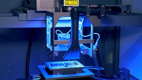
3.2 Photoresist Coating
The liquid photoresist is applied using one of the following methods:
- Spin coating: Uniform distribution via high-speed spinning (common in IC fabrication).
- Curtain coating: Continuous liquid flow for high-throughput production.
- Spray coating: Suitable for irregular surfaces but less precise.
- Dip coating: Immersion of the substrate into the photoresist solution.
After coating, the PCB is pre-baked (typically at 70–90°C) to evaporate solvents and solidify the film.
3.3 Exposure
The coated PCB is exposed to UV light through a photomask (film or glass) containing the circuit pattern. Areas exposed to UV light polymerize and become insoluble in the developer, while unexposed regions remain soluble.
Key exposure parameters:
- UV wavelength: 365–405 nm
- Exposure energy: 100–300 mJ/cm² (varies with photoresist type)
- Alignment accuracy: Critical for high-density interconnect (HDI) PCBs
3.4 Development
The PCB is immersed in a developer solution (usually sodium carbonate or potassium carbonate), which dissolves the unexposed photoresist, revealing the copper underneath. Development time and concentration must be carefully controlled to avoid over- or under-development.
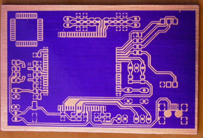
3.5 Etching
The developed PCB undergoes etching to remove unprotected copper. Common etchants include:
- Ferric chloride (FeCl₃) – Traditional, cost-effective
- Ammonium persulfate ((NH₄)₂S₂O₈) – Less corrosive
- Cupric chloride (CuCl₂) – Regenerative, used in high-volume production
The etching process must be monitored to prevent undercutting or over-etching.
3.6 Stripping
After etching, the remaining photoresist is stripped using an alkaline solution (e.g., sodium hydroxide). The PCB is then rinsed and dried, completing the pattern transfer process.
4. Advantages of Wet Film Process
- Higher resolution: Capable of producing finer traces (< 25 µm) compared to dry film.
- Better conformality: Adapts well to uneven surfaces and small vias.
- Cost-effective for small batches: No need for expensive lamination equipment.
- Thinner resist layers: Enables precise etching control.
5. Disadvantages and Challenges
- Process complexity: Requires precise control of coating, exposure, and development.
- Environmental concerns: Chemical disposal (developers, strippers) must be managed.
- Lower throughput: Slower than dry film for mass production.
- Defect sensitivity: Dust and bubbles can cause pinholes or adhesion failures.
6. Comparison with Dry Film Photoresist
| Parameter | Wet Film | Dry Film |
|---|---|---|
| Resolution | < 25 µm | 50–75 µm |
| Adhesion | Excellent on smooth copper | Good, but may lift on rough surfaces |
| Process Speed | Slower | Faster (automated lamination) |
| Cost | Lower for small batches | Higher initial investment |
| Thickness Control | More precise | Limited by film thickness |
7. Applications of Wet Film in PCB Manufacturing
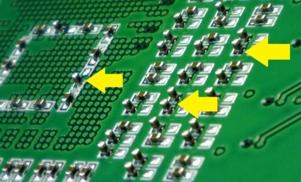
- High-density interconnect (HDI) PCBs – Smartphones, wearables
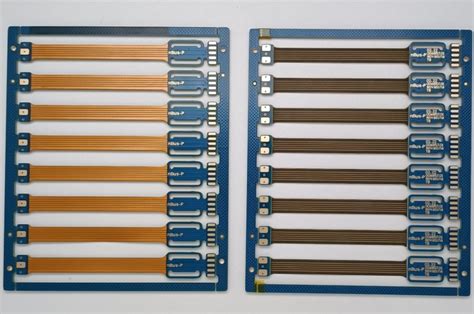
- Flexible PCBs – Medical devices, automotive electronics
- RF/microwave PCBs – High-frequency signal integrity
- Fine-pitch IC substrates – Advanced packaging
8. Future Trends and Improvements
- Water-developable photoresists – Reducing chemical waste
- Advanced coating techniques – Inkjet printing for digital patterning
- Hybrid processes – Combining wet and dry film for optimal performance
9. Conclusion
The wet film process remains a vital technique in PCB manufacturing, particularly for high-precision applications. While it demands careful process control, its superior resolution and cost efficiency make it indispensable for prototyping and fine-line PCBs. As technology advances, innovations in photoresist chemistry and application methods will further enhance its role in electronics production.