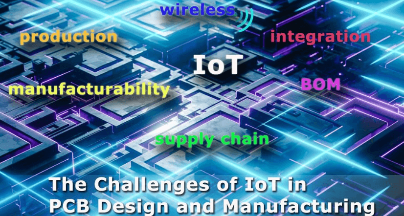
IoT PCB Design Challenge: Overcoming the Complexities of Modern Electronics
Introduction
The Internet of Things (IoT) has revolutionized the way we interact with technology, embedding intelligence into everyday objects—from smart home devices to industrial sensors. At the heart of every IoT device lies a printed circuit board (PCB), which serves as the foundation for functionality, connectivity, and power management. However, designing PCBs for IoT applications presents unique challenges due to the demand for miniaturization, low power consumption, wireless connectivity, and reliability.
The IoT PCB Design Challenge is an initiative that encourages engineers and designers to push the boundaries of PCB technology to meet the evolving demands of IoT devices. This article explores the key challenges in IoT PCB design, innovative solutions, and the future of PCB development in the IoT ecosystem.
Key Challenges in IoT PCB Design
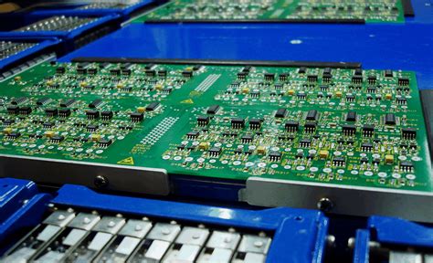
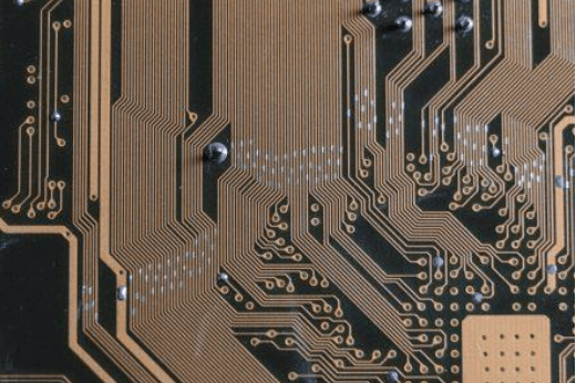
1. Miniaturization and High-Density Layouts
IoT devices are becoming increasingly compact, requiring PCBs to fit into small form factors while maintaining high performance. This demands:
- High-density interconnect (HDI) PCBs with microvias and fine-pitch components.
- Multilayer stack-ups to accommodate complex routing without increasing board size.
- Embedded components to save space and reduce parasitic effects.
Challenge: Ensuring signal integrity and thermal management in tightly packed designs.
2. Low Power Consumption
Many IoT devices operate on batteries or energy harvesting, making power efficiency critical. Design considerations include:
- Ultra-low-power microcontrollers (e.g., ARM Cortex-M series).
- Efficient power management ICs (PMICs) with dynamic voltage scaling.
- Optimized sleep modes to extend battery life.
Challenge: Balancing performance with power constraints, especially in always-on devices.
3. Wireless Connectivity Integration
IoT devices rely on wireless protocols such as Wi-Fi, Bluetooth, Zigbee, LoRa, and cellular (NB-IoT, LTE-M). PCB design must account for:
- Antenna placement and tuning to avoid interference.
- RF shielding to prevent noise from affecting sensitive components.
- Impedance matching for high-frequency signals.
Challenge: Maintaining strong signal strength while minimizing interference in compact designs.
4. Thermal Management
Heat dissipation is critical in small IoT devices with high-power components. Solutions include:
- Thermal vias to transfer heat away from hotspots.
- Heat sinks and conductive materials for passive cooling.
- Optimized component placement to avoid thermal coupling.
Challenge: Preventing overheating without increasing PCB size or cost.
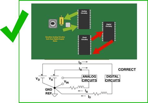
5. EMI/EMC Compliance
IoT devices must comply with electromagnetic interference (EMI) and electromagnetic compatibility (EMC) standards. Key strategies:
- Proper grounding techniques (star grounding, ground planes).
- Shielding cans for sensitive RF sections.
- Careful routing of high-speed signals to minimize crosstalk.
Challenge: Passing regulatory certifications (FCC, CE) while maintaining performance.
6. Reliability and Durability
IoT devices often operate in harsh environments (industrial, outdoor, medical). Design considerations:
- Conformal coating to protect against moisture and dust.
- Robust materials (high-Tg PCBs, flexible circuits for wearables).
- Vibration-resistant soldering (e.g., underfill for BGA components).
Challenge: Ensuring long-term reliability without significant cost increases.
7. Security Considerations
IoT devices are vulnerable to cyber threats. Hardware security measures include:
- Secure boot MCUs with cryptographic accelerators.
- Tamper-resistant PCB designs (e.g., mesh shields against physical attacks).
- Isolated power domains to prevent side-channel attacks.
Challenge: Implementing security without compromising performance or cost.
Innovative Solutions in IoT PCB Design
1. Advanced PCB Materials
- Flex and Rigid-Flex PCBs: Enable compact, bendable designs for wearables and medical devices.
- Low-Loss Dielectrics: Improve signal integrity for high-frequency RF applications.
- Embedded Passive Components: Reduce board space and improve performance.
2. AI-Assisted PCB Design
- Automated Routing Tools: Use machine learning to optimize trace layouts for EMI and signal integrity.
- Thermal Simulation Software: Predict hotspots and optimize component placement.
3. Modular Design Approaches
- System-on-Module (SoM) Solutions: Pre-certified wireless modules (e.g., ESP32, Nordic nRF) reduce design complexity.
- Breakout Boards for Prototyping: Accelerate development with standardized interfaces.
4. Energy Harvesting Techniques
- Solar-Powered PCBs: Integrate thin-film solar cells for self-sustaining devices.
- RF Energy Harvesting: Capture ambient wireless signals for low-power sensors.
5. 3D Printing for Rapid Prototyping
- Additive Manufacturing: Enables quick iteration of PCB designs with complex geometries.
- Embedded Electronics: 3D-printed circuits with integrated components.
The Future of IoT PCB Design
As IoT continues to expand, PCB design will evolve with trends such as:
- 5G-Enabled IoT: Higher-frequency PCBs with mmWave support.
- Edge AI Processing: More powerful processors requiring advanced thermal solutions.
- Sustainable Electronics: Eco-friendly materials and recyclable PCBs.
- Quantum Computing Interfaces: Novel PCB architectures for quantum IoT devices.
The IoT PCB Design Challenge will remain a driving force for innovation, pushing engineers to develop smarter, more efficient, and more reliable solutions.
Conclusion
Designing PCBs for IoT applications is a complex yet rewarding challenge. Engineers must balance miniaturization, power efficiency, wireless connectivity, thermal management, and security while meeting industry standards. Through advanced materials, AI-driven design tools, and modular approaches, the future of IoT PCB design looks promising.
The IoT PCB Design Challenge serves as a catalyst for breakthroughs in electronics, ensuring that IoT devices continue to transform industries and improve our daily lives. As technology advances, so too will the ingenuity of PCB designers in overcoming these challenges.
Are you ready to take on the challenge?