Jablotron pcb assembly
Understanding the Basics of Jablotron PCB Assembly
Jablotron, a renowned name in the field of security systems and electronic devices, has made significant strides in the development and assembly of printed circuit boards (PCBs). Understanding the basics of Jablotron PCB assembly is crucial for those interested in the intricacies of electronic manufacturing and design. At the heart of any electronic device, PCBs serve as the foundational platform that connects and supports various electronic components. Jablotron’s approach to PCB assembly is characterized by precision, innovation, and adherence to high-quality standards, ensuring the reliability and efficiency of their product
To begin with, the PCB assembly process involves several critical stages, each requiring meticulous attention to detail.
Initially, the design phase is paramount, where engineers utilize advanced software tools to create a schematic layout of the circuit. This blueprint serves as a guide for the subsequent stages of assembly. Jablotron places a strong emphasis on this phase, ensuring that the design is both functional and optimized for performance. Once the design is finalized, the next step involves the fabrication of the PCB itself. This process includes the etching of copper layers onto a non-conductive substrate, creating the necessary pathways for electrical currents.
Following fabrication, the assembly process moves to the placement of components.
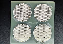
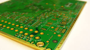
Surface mount technology (SMT) is predominantly used in Jablotron’s PCB assembly, allowing for the efficient and precise placement of components onto the board. This method not only enhances the compactness of the design but also improves the overall performance of the device. During this stage, automated machines are employed to place components such as resistors, capacitors, and integrated circuits onto the board with remarkable accuracy. The use of automation in this process minimizes human error and ensures consistency across large production volumes.
Once the components are placed, the next critical step is soldering, which secures the components to the PCB.
Jablotron employs advanced soldering techniques, such as reflow soldering, to achieve strong and reliable connections. This process involves heating the board to a specific temperature, causing the solder paste to melt and form a bond between the components and the board. The precision of this process is vital, as any defects in soldering can lead to malfunctioning devices.
After soldering, the assembled PCBs undergo rigorous testing to ensure their functionality and reliability.
Jablotron implements a variety of testing methods, including automated optical inspection (AOI) and in-circuit testing (ICT), to detect any defects or irregularities. These tests are crucial in maintaining the high standards of quality that Jablotron is known for. By identifying and rectifying any issues at this stage, Jablotron ensures that only fully functional and reliable products reach the market.
In conclusion, understanding the basics of Jablotron PCB assembly provides valuable insight into the meticulous processes involved in creating high-quality electronic devices. From the initial design phase to the final testing stage, each step is executed with precision and care. Jablotron’s commitment to innovation and quality is evident in their approach to PCB assembly, making them a leader in the field of electronic manufacturing. As technology continues to evolve, Jablotron remains at the forefront, consistently delivering reliable and efficient solutions to meet the demands of an ever-changing market.
Key Challenges in Jablotron PCB Assembly and How to Overcome Them
Jablotron, a renowned name in the field of electronic security systems, relies heavily on the precision and reliability of its printed circuit board (PCB) assemblies. The process of assembling PCBs for Jablotron products is fraught with challenges that can impact both the functionality and durability of the final product. Understanding these challenges and implementing strategies to overcome them is crucial for maintaining the high standards associated with the Jablotron brand.
One of the primary challenges in Jablotron PCB assembly is ensuring the accuracy of component placement.
Given the complexity and miniaturization of modern electronic components, even a slight misalignment can lead to significant performance issues or complete device failure. To address this, manufacturers often employ advanced automated pick-and-place machines that use sophisticated vision systems to ensure precise component placement. Additionally, regular calibration and maintenance of these machines are essential to maintain their accuracy over time.
Another significant challenge is the soldering process, which is critical for establishing reliable electrical connections between components and the PCB.
Inadequate soldering can result in weak joints that may fail under stress or thermal cycling. To mitigate this risk, manufacturers can utilize reflow soldering techniques, which provide consistent heat distribution and controlled cooling rates, thereby enhancing the quality of solder joints. Moreover, implementing rigorous inspection protocols, such as automated optical inspection (AOI) and X-ray inspection, can help identify soldering defects early in the production process.
Thermal management is also a crucial consideration in Jablotron PCB assembly.
As electronic devices become more powerful, they generate more heat, which can adversely affect performance and longevity. Effective thermal management strategies, such as the use of heat sinks, thermal vias, and appropriate PCB materials, are essential to dissipate heat efficiently. Additionally, conducting thermal simulations during the design phase can help identify potential hotspots and optimize the layout for better heat distribution.
Furthermore, the increasing complexity of Jablotron products necessitates the integration of multiple functionalities onto a single PCB.
This integration can lead to electromagnetic interference (EMI) issues, which can degrade the performance of the device. To combat EMI, designers can employ techniques such as proper grounding, the use of shielding materials, and careful routing of signal traces. Additionally, adhering to industry standards and guidelines for EMI control can further enhance the electromagnetic compatibility of the PCB.
Supply chain management poses another challenge in the assembly of Jablotron PCBs.
The availability of high-quality components is critical to ensure the reliability of the final product. However, fluctuations in the global supply chain can lead to component shortages or delays. To mitigate these risks, manufacturers can establish strong relationships with multiple suppliers and maintain a strategic inventory of critical components. Additionally, adopting a flexible design approach that allows for the use of alternative components can provide a buffer against supply chain disruptions.
In conclusion, while the assembly of Jablotron PCBs presents several challenges, a combination of advanced technology, meticulous planning, and strategic management can effectively address these issues.
By focusing on precision in component placement, ensuring robust soldering processes, implementing effective thermal management, controlling electromagnetic interference, and managing supply chain risks, manufacturers can uphold the quality and reliability that Jablotron products are known for. Through these efforts, the integrity and performance of Jablotron’s electronic security systems can be maintained, ensuring customer satisfaction and trust in the brand.
Innovations in Jablotron PCB Assembly Technology
Jablotron, a renowned name in the field of electronic security systems, has consistently been at the forefront of technological innovation. One of the critical areas where Jablotron has demonstrated significant advancements is in printed circuit board (PCB) assembly technology. This process, which involves the mounting of electronic components onto a PCB, is crucial for the functionality and reliability of electronic devices. As the demand for more sophisticated and compact security systems grows, Jablotron has embraced cutting-edge technologies to enhance the efficiency and precision of its PCB assembly processes.
To begin with, Jablotron has integrated advanced surface mount technology (SMT) into its PCB assembly operations.
SMT allows for the placement of components directly onto the surface of the PCB, as opposed to the traditional through-hole method, which requires inserting component leads into drilled holes. This transition to SMT has enabled Jablotron to produce more compact and lightweight devices, which are essential for modern security systems that require discreet installation and operation. Moreover, SMT facilitates higher component density, allowing for more complex circuitry within a smaller footprint, thereby enhancing the functionality of Jablotron’s products.
In addition to SMT, Jablotron has adopted automated optical inspection (AOI) systems to ensure the quality and accuracy of its PCB assemblies.
AOI systems use high-resolution cameras and sophisticated algorithms to inspect PCBs for defects such as misaligned components, soldering errors, and other anomalies. By implementing AOI, Jablotron can detect and rectify potential issues early in the production process, thereby reducing the likelihood of defective products reaching the market. This commitment to quality assurance not only enhances the reliability of Jablotron’s security systems but also reinforces the company’s reputation for excellence.
Furthermore, Jablotron has embraced the use of advanced materials in its PCB assembly processes.
The selection of high-quality substrates and soldering materials is crucial for ensuring the durability and performance of PCBs, especially in security systems that may be exposed to harsh environmental conditions. By utilizing materials with superior thermal and electrical properties, Jablotron ensures that its PCBs can withstand the rigors of real-world applications, providing customers with peace of mind regarding the longevity and dependability of their security systems.
Another noteworthy innovation in Jablotron’s PCB assembly technology is the implementation of environmentally friendly practices.
The company has made concerted efforts to minimize the environmental impact of its manufacturing processes by adopting lead-free soldering techniques and reducing waste through efficient material usage. These initiatives align with global trends towards sustainability and demonstrate Jablotron’s commitment to responsible manufacturing practices.
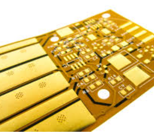
Moreover, Jablotron’s investment in research and development has led to the exploration of emerging technologies such as flexible PCBs and 3D printing.
Flexible PCBs offer the advantage of being bendable and adaptable to various shapes, which can be particularly beneficial for security systems that require installation in unconventional spaces. Meanwhile, 3D printing holds the potential to revolutionize PCB prototyping and production by enabling rapid iteration and customization.
In conclusion, Jablotron’s innovations in PCB assembly technology underscore the company’s dedication to advancing the capabilities and reliability of its electronic security systems. By leveraging state-of-the-art techniques such as surface mount technology, automated optical inspection, and the use of advanced materials, Jablotron continues to set new standards in the industry. As the company explores emerging technologies and embraces sustainable practices, it remains well-positioned to meet the evolving needs of its customers while maintaining its leadership in the field of electronic security.
The Future of Jablotron PCB Assembly: Trends to Watch
The future of Jablotron PCB assembly is poised for significant transformation, driven by technological advancements and evolving industry demands. As we delve into the trends shaping this sector, it becomes evident that innovation is at the forefront, promising enhanced efficiency, precision, and functionality.
One of the most notable trends is the increasing integration of automation in PCB assembly processes.
Automation not only accelerates production timelines but also minimizes human error, ensuring higher quality and consistency in the final products. This shift towards automated systems is further complemented by the adoption of advanced robotics, which enhances the precision of component placement and soldering, thereby improving the overall reliability of the assemblies.
In addition to automation, the rise of the Internet of Things (IoT) is significantly influencing Jablotron PCB assembly.
As IoT devices proliferate, there is a growing demand for PCBs that can support complex functionalities while maintaining compact form factors. This necessitates the development of multi-layered PCBs with increased component density, a challenge that manufacturers are addressing through innovative design and fabrication techniques. Moreover, the need for PCBs that can withstand diverse environmental conditions is prompting the use of advanced materials and coatings, ensuring durability and performance in various applications.
Another trend to watch is the emphasis on sustainability within the PCB assembly industry.
As environmental concerns gain prominence, there is a concerted effort to reduce the ecological footprint of manufacturing processes. This includes the adoption of eco-friendly materials, energy-efficient production methods, and recycling initiatives aimed at minimizing waste. By prioritizing sustainability, Jablotron and other industry players are not only meeting regulatory requirements but also aligning with the growing consumer preference for environmentally responsible products.
Furthermore, the advent of Industry 4.0 is revolutionizing PCB assembly through the integration of smart technologies.
The use of data analytics, machine learning, and artificial intelligence is enabling manufacturers to optimize production processes, predict maintenance needs, and enhance quality control. These technologies facilitate real-time monitoring and decision-making, allowing for more agile and responsive manufacturing operations. As a result, companies can better meet the dynamic demands of the market while maintaining high standards of quality and efficiency.
In parallel, the globalization of supply chains is influencing the future of Jablotron PCB assembly.
With components sourced from various parts of the world, there is an increased focus on supply chain resilience and risk management. Manufacturers are investing in digital tools to enhance supply chain visibility and agility, ensuring that disruptions are minimized and production schedules are maintained. This global perspective also encourages collaboration and knowledge sharing across borders, fostering innovation and driving the industry forward.
Lastly, the continuous evolution of consumer electronics is shaping the requirements for PCB assembly.
As devices become more sophisticated, there is a demand for PCBs that can support advanced functionalities such as high-speed data processing, wireless connectivity, and enhanced power management. This trend is pushing the boundaries of PCB design and assembly, prompting manufacturers to explore new technologies and methodologies to meet these complex requirements.
In conclusion, the future of Jablotron PCB assembly is characterized by a confluence of technological advancements and industry trends that promise to redefine the landscape. From automation and IoT integration to sustainability and smart manufacturing, these developments are setting the stage for a more efficient, innovative, and responsive industry. As these trends continue to unfold, they will undoubtedly shape the trajectory of PCB assembly, offering exciting opportunities and challenges for manufacturers and stakeholders alike.