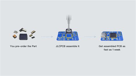
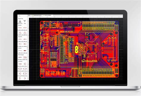
JLCPCB PCB Assembly: Optimized Electronics Production Solutions

Key Takeaways
Modern electronics manufacturing demands PCB assembly solutions that balance speed, cost, and precision. JLCPCB’s turnkey services integrate PCBA workflows to reduce bottlenecks in prototyping and mass production. By combining automated processes with rigorous quality checks, they ensure consistent output for both low-volume and high-volume orders. A standout advantage is their real-time component sourcing, which minimizes delays caused by supply chain disruptions. Engineers benefit from rapid prototyping cycles, enabling iterative testing without compromising timelines. For bulk orders, optimized panelization and material utilization lower per-unit costs while maintaining IPC-A-610 compliance. Advanced PCB assembly technologies, such as automated optical inspection (AOI), detect defects early, reducing rework and ensuring reliability. Additionally, JLCPCB’s cloud-based platform streamlines order tracking, simplifying communication across global teams. Whether scaling prototypes or managing large-scale production, their PCBA solutions prioritize time-to-market efficiency without sacrificing performance standards. This approach positions JLCPCB as a strategic partner for businesses navigating competitive electronics markets.
JLCPCB Assembly Services for Electronics Manufacturing
Modern electronics manufacturing demands PCB assembly solutions that balance precision, speed, and scalability. JLCPCB’s PCBA services address these needs by integrating advanced automation with rigorous quality protocols, enabling seamless transitions from prototyping to mass production. Their platform supports design-for-manufacturability (DFM) analysis, minimizing errors and ensuring compatibility with high-speed pick-and-place systems.
For prototyping, JLCPCB offers 24-hour turnaround times, allowing engineers to validate designs rapidly. Bulk orders benefit from optimized material procurement and panelization strategies, reducing per-unit costs by up to 30% in high-volume scenarios.
| Service Feature | Prototyping | Bulk Production |
|---|---|---|
| Lead Time | 24–72 hours | 5–10 days |
| Component Sourcing | Partial/Full Turnkey | Full Turnkey Only |
| Quality Checks | 3-stage inspection | 6-stage inspection |
“JLCPCB’s assembly workflows eliminate bottlenecks common in traditional PCB manufacturing, particularly for complex multi-layer designs.” – Senior Embedded Systems Engineer
The company’s turnkey PCBA approach simplifies logistics by managing everything from component procurement to final testing. By leveraging real-time inventory tracking and automated assembly lines, JLCPCB ensures consistent output even for orders exceeding 10,000 units. This scalability, combined with ISO-certified processes, positions their PCB assembly services as a strategic asset for startups and enterprises alike.
Cost-Effective PCB Assembly Solutions by JLCPCB
In today’s competitive electronics market, balancing quality with affordability is critical. JLCPCB addresses this challenge through its optimized PCB assembly workflows, which leverage economies of scale and advanced automation to reduce costs without compromising reliability. By integrating PCBA services with in-house fabrication, the company eliminates third-party dependencies, streamlining material procurement and minimizing overhead. This approach enables cost savings of up to 30% compared to traditional assembly methods, particularly for mid- to high-volume orders.
A key advantage lies in JLCPCB’s transparent pricing model, which factors in component sourcing, board fabrication, and assembly labor into a single quote. Clients benefit from real-time cost calculators that adjust based on design complexity, layer counts, and solder mask options. For projects requiring cost-effective PCB assembly, the platform supports both standard and custom specifications, including lead-free finishes and industrial-grade IC mounting. Additionally, bulk order discounts and bundled shipping options further enhance affordability for recurring production cycles.
By prioritizing scalable solutions, JLCPCB ensures that startups and enterprises alike can access professional-grade PCBA services tailored to budget constraints. Whether prototyping or scaling to mass production, their hybrid model combines automated pick-and-place systems with rigorous quality checks, ensuring consistent performance across every batch. This balance of precision and affordability makes JLCPCB a strategic partner for developers aiming to accelerate time-to-market while maintaining financial efficiency.
Rapid Prototyping With JLCPCB’s PCB Assembly
For engineers and designers prioritizing speed without compromising quality, JLCPCB’s PCB assembly services offer a streamlined pathway from concept to functional prototype. By integrating advanced PCBA workflows with automated manufacturing systems, the platform reduces turnaround times to as little as 24 hours for design verification. This agility is critical for iterative development cycles, enabling rapid testing of circuit functionality and form-factor compatibility.
A key advantage lies in JLCPCB’s component sourcing network, which minimizes delays by providing access to over 200,000 verified parts. This ensures that even complex PCB assembly projects maintain momentum during prototyping phases. Additionally, the platform’s design rule checks (DRCs) and real-time pricing tools help avoid costly revisions, aligning prototype iterations with budget constraints.
For startups and R&D teams, JLCPCB’s support for small-batch PCBA orders allows cost-effective validation of designs before scaling production. The combination of precision assembly techniques and rigorous quality controls ensures prototypes mirror the reliability of mass-produced boards. This seamless transition from prototype to bulk manufacturing positions JLCPCB as a strategic partner for innovators navigating tight timelines.
Bulk Order Optimization Using JLCPCB Assembly
For electronics manufacturers scaling production, PCB assembly efficiency becomes critical. JLCPCB’s bulk-order optimization leverages automated processes and economies of scale to reduce per-unit costs while maintaining consistency. By integrating PCBA workflows with advanced inventory management systems, the platform ensures seamless material sourcing, minimizing delays for high-volume orders.
A key advantage lies in JLCPCB’s component procurement network, which negotiates competitive pricing for common parts through supplier partnerships. This directly lowers expenses for recurring projects, particularly when paired with their design-for-manufacturability (DFM) checks to eliminate errors early. For example, standardized panelization techniques maximize material usage, cutting waste by up to 15% in large batches.
Transitioning from prototyping to mass production is streamlined through JLCPCB’s turnkey solutions, which unify fabrication, PCB assembly, and testing. Automated optical inspection (AOI) systems maintain defect rates below 0.1%, even under accelerated timelines. Additionally, their API-driven ordering system allows enterprises to synchronize production schedules with real-time demand, reducing overstock risks.
By adopting just-in-time manufacturing principles, JLCPCB enables clients to scale PCBA output without compromising turnaround speeds—ideal for industries like consumer electronics or IoT devices requiring rapid market deployment. This balance of precision, scalability, and cost control positions bulk orders for sustainable growth.
Precision PCB Assembly for Reliable Electronics
Modern electronics demand PCB assembly processes that prioritize accuracy and repeatability to ensure end-product reliability. Advanced surface-mount technology (SMT) and automated optical inspection (AOI) systems enable manufacturers to achieve micron-level placement accuracy, critical for high-density designs. By integrating PCBA workflows with rigorous testing protocols, production teams can identify defects like solder bridging or component misalignment early, minimizing post-assembly rework.
For mission-critical applications—such as medical devices or aerospace systems—the tolerance for error approaches zero. Here, controlled impedance routing and thermal management become pivotal design considerations. Automated pick-and-place machines, paired with precision stenciling techniques, ensure consistent solder paste application, while X-ray inspection verifies hidden connections in multilayer boards. This meticulous approach reduces field failure rates and extends product lifespans.
Scalability remains integral to precision-focused PCB assembly, allowing seamless transitions from prototype validation to volume manufacturing. By standardizing design rules and material specifications, manufacturers maintain uniformity across batches without compromising speed. Such optimization aligns with industries requiring both technical excellence and supply chain predictability, reinforcing the role of precision in building trustworthy electronic ecosystems.
Streamlined Production With JLCPCB Assembly Tech
Modern electronics manufacturing demands PCB assembly processes that eliminate bottlenecks while maintaining precision. JLCPCB addresses this through integrated PCBA workflows combining automated component sourcing, assembly line optimization, and real-time quality monitoring. By synchronizing design files with their proprietary manufacturing execution system (MES), the platform minimizes manual interventions, ensuring consistent material traceability and process repeatability.
A key advantage lies in JLCPCB’s use of high-speed pick-and-place machines coupled with automated optical inspection (AOI). These technologies enable rapid placement of surface-mount devices (SMDs) with micrometer-level accuracy, reducing assembly cycles by up to 40% compared to conventional methods. For complex projects, the dynamic supply chain network ensures critical components are pre-vetted and available, mitigating delays.
The PCBA ecosystem also supports scalable production, allowing seamless transitions from low-volume prototyping to high-volume runs. Engineers benefit from cloud-based project management tools that track progress across fabrication, assembly, and testing phases. This end-to-digitization not only accelerates time-to-market but also aligns with lean manufacturing principles, cutting waste in material usage and labor costs. By standardizing these workflows, JLCPCB establishes a blueprint for agile electronics production adaptable to evolving industry demands.
JLCPCB’s Turnkey Solutions for PCB Manufacturing
For manufacturers seeking end-to-end efficiency, JLCPCB’s turnkey PCB assembly services eliminate logistical complexities by integrating design, component sourcing, and production into a unified workflow. By managing every stage—from PCBA design verification to final testing—the platform ensures seamless transitions between prototyping and mass production. Advanced automation tools optimize material procurement, reducing lead times by up to 30% compared to traditional fragmented workflows.
A key advantage lies in JLCPCB’s curated inventory of over 200,000 certified components, which minimizes procurement delays and ensures compatibility for complex PCB assembly projects. Their cloud-based quoting system enables real-time cost analysis, allowing engineers to balance budget constraints with performance requirements. For high-volume orders, the platform’s scalable manufacturing infrastructure guarantees consistent output quality through AI-driven process monitoring and precision placement machinery.
Moreover, JLCPCB’s turnkey model supports design-for-manufacturing (DFM) checks, identifying potential flaws early to prevent costly revisions. This proactive approach, combined with ISO-certified PCBA testing protocols, ensures reliability across industrial, automotive, and consumer electronics applications. By consolidating supply chain dependencies and leveraging economies of scale, businesses achieve faster market entry without compromising on PCB assembly precision or compliance standards.
Quality Assurance in JLCPCB PCB Assembly Process
Central to the reliability of PCB assembly services is a rigorous quality assurance (QA) framework. JLCPCB’s PCBA workflows integrate automated optical inspection (AOI) systems to detect soldering defects, component misalignment, or trace inconsistencies at micron-level precision. Advanced X-ray inspection further validates hidden connections in multilayer boards, ensuring structural integrity even for high-density designs. To maintain consistency, every batch undergoes functional testing under simulated operating conditions, verifying performance metrics like power efficiency and signal stability.
Adherence to IPC-A-610/620 standards governs material selection and assembly protocols, minimizing risks of thermal stress or electrical failure. The QA process also includes traceability protocols, with serialized tracking for critical components to streamline troubleshooting and compliance reporting. By combining automated precision with human oversight, JLCPCB reduces error rates to below 0.1% across prototyping and bulk orders. This multi-layered approach not only safeguards product longevity but also accelerates time-to-market by preempting rework cycles—a critical advantage in industries demanding zero-tolerance for defects.
Conclusion
In modern electronics manufacturing, achieving optimal balance between speed, cost, and quality remains a critical challenge. PCB assembly services, particularly PCBA solutions from JLCPCB, address these demands by integrating advanced automation and rigorous quality protocols. By leveraging economies of scale and standardized workflows, manufacturers can minimize production delays while maintaining cost predictability—a vital factor for startups and enterprises alike.
The adaptability of PCBA processes also supports seamless transitions from prototyping to large-scale manufacturing, ensuring design integrity across all stages. JLCPCB’s emphasis on precision engineering reduces error margins, which is essential for applications requiring high reliability, such as medical devices or industrial systems. Furthermore, their turnkey approach simplifies supply chain coordination, enabling clients to focus on innovation rather than logistical complexities.
As industries increasingly prioritize agility and sustainability, partnering with providers offering scalable PCB assembly solutions becomes a strategic advantage. By aligning technical expertise with operational efficiency, JLCPCB exemplifies how modern electronics production can evolve to meet both current and emerging market demands.
Frequently Asked Questions
What file formats does JLCPCB accept for PCB assembly orders?
JLCPCB supports standard formats such as Gerber files (RS-274X), Bill of Materials (BOM), and Centroid files (Pick-and-Place). Ensure your design files include clear layer labeling and component specifications to streamline the PCBA process.
How does JLCPCB ensure quality in high-volume PCB assembly?
The company employs automated optical inspection (AOI), X-ray testing, and functional testing for bulk orders. Combined with ISO-certified workflows, this guarantees consistent reliability across prototypes and mass production runs.
What components are included in JLCPCB’s turnkey PCB assembly service?
Their turnkey solution covers PCB fabrication, component sourcing, assembly, and testing. Clients benefit from end-to-end coordination, reducing logistical delays and minimizing risks of component mismatches during PCBA.
Can JLCPCB handle both prototype and bulk PCB assembly requests?
Yes, JLCPCB optimizes its production lines for rapid prototyping (24-hour turnaround) and cost-effective bulk orders. Flexible MOQs and tiered pricing make it suitable for startups and enterprises alike.
How are shipping costs calculated for assembled PCBs?
Shipping fees depend on order volume, destination, and delivery speed. JLCPCB offers multiple logistics partners, allowing clients to balance cost efficiency and urgency for their PCB assembly projects.
Ready to Start Your Next Project?
For tailored PCB assembly solutions or to request a real-time quote, please click here. Explore how JLCPCB’s expertise can accelerate your electronics manufacturing workflow.