Key Challenges in the PCB Assembly Process
Printed Circuit Board (PCB) assembly is a critical stage in electronics manufacturing, where components are mounted onto the board to create functional circuits. Despite advancements in technology, the PCB assembly process still faces several challenges that can affect product quality, reliability, and production efficiency. This article explores the major challenges encountered during PCB assembly and discusses potential solutions to mitigate them.
1. Component Miniaturization and High-Density Designs
Challenge:
With the increasing demand for smaller and more powerful electronic devices, PCB designs have become more complex, featuring high-density interconnects (HDI) and miniature components such as 0201, 01005, and even smaller chip-scale packages (CSPs). This miniaturization poses several difficulties:
- Placement Accuracy: Tiny components require ultra-precise pick-and-place machines to avoid misalignment.
- Solder Bridging: Closely spaced pads increase the risk of solder bridging, leading to short circuits.
- Inspection Difficulties: Visual inspection becomes challenging, necessitating advanced automated optical inspection (AOI) and X-ray inspection systems.
Solution:
- Use high-precision assembly equipment with vision systems for accurate component placement.
- Implement advanced solder paste printing techniques, such as laser stencil cutting, to ensure precise deposition.
- Employ 3D AOI and X-ray inspection to detect defects in densely packed boards.
2. Solder Paste Application and Stencil Printing Issues
Challenge:
Solder paste printing is a critical step in surface-mount technology (SMT) assembly. Common issues include:
- Inconsistent Solder Paste Deposition: Poor stencil design, clogged apertures, or improper squeegee pressure can lead to insufficient or excessive solder paste.
- Solder Balling: Caused by moisture absorption or improper reflow profiles, leading to small solder balls that can cause short circuits.
- Paste Slumping: Solder paste spreads beyond the pad area before reflow, increasing the risk of bridging.
Solution:
- Optimize stencil design with proper aperture size and shape.
- Maintain controlled environmental conditions (humidity and temperature) to prevent paste degradation.
- Use high-quality solder paste with appropriate viscosity and metal content.
- Implement real-time solder paste inspection (SPI) systems to detect defects early.
3. Thermal Management During Reflow Soldering
Challenge:
Reflow soldering involves heating the PCB to melt solder paste and form reliable joints. However, thermal challenges include:
- Thermal Imbalance: Large and small components on the same board may heat unevenly, leading to cold joints or component damage.
- Thermal Shock: Rapid temperature changes can crack components or PCB substrates.
- Warping: Excessive heat can cause PCB warping, leading to misalignment and open solder joints.
Solution:
- Optimize reflow profiles based on component specifications and PCB material.
- Use zone-controlled reflow ovens to ensure uniform heating.
- Implement preheating stages to minimize thermal shock.
- Select PCB materials with high thermal stability (e.g., polyimide for flexible PCBs).
4. Component Availability and Supply Chain Disruptions
Challenge:
The electronics industry frequently faces shortages of critical components due to:
- Global Supply Chain Issues: Geopolitical tensions, pandemics, and natural disasters disrupt component availability.
- Obsolescence: Some components become obsolete quickly, forcing last-time buys (LTB) or redesigns.
- Counterfeit Parts: Fake or substandard components can lead to failures in the field.
Solution:
- Maintain strong relationships with multiple suppliers to reduce dependency on a single source.
- Use component lifecycle management tools to anticipate obsolescence.
- Implement strict counterfeit detection measures, such as X-ray fluorescence (XRF) testing.
- Consider alternative components or redesigns early in the product lifecycle.
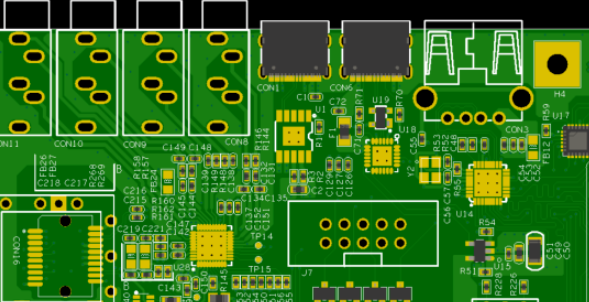
5. Mixed-Technology Assembly (SMT + Through-Hole)
Challenge:
Many PCBs require both surface-mount (SMT) and through-hole (THT) components, introducing complications such as:
- Process Complexity: Different soldering techniques (reflow for SMT, wave soldering for THT) increase production steps.
- Mechanical Stress: Manual insertion of THT components can damage nearby SMT parts.
- Selective Soldering Challenges: High-pin-count connectors and large components may require selective soldering, which is time-consuming.
Solution:
- Use automated insertion machines for THT components where possible.
- Implement selective soldering systems for precise application.
- Optimize assembly sequence to minimize handling risks.
6. Quality Control and Defect Detection
Challenge:
Ensuring defect-free PCB assemblies is critical but challenging due to:
- Hidden Defects: Issues like voids in ball grid array (BGA) solder joints are not visible without X-ray inspection.
- False Calls in AOI: Overly sensitive inspection systems may flag acceptable variations as defects, increasing rework.
- Human Error in Manual Inspection: Fatigue and subjectivity can lead to missed defects.
Solution:
- Combine multiple inspection methods (AOI, X-ray, and functional testing).
- Use AI-powered inspection systems to reduce false positives.
- Implement statistical process control (SPC) to monitor production trends.
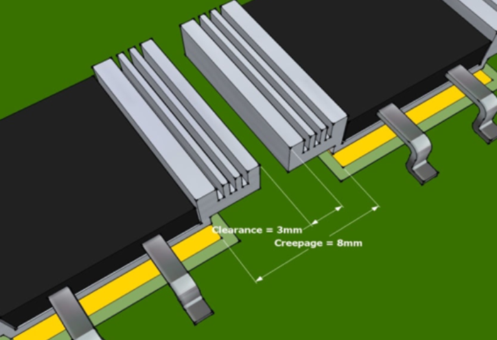
7. Environmental and Regulatory Compliance
Challenge:
PCB assembly must comply with environmental regulations such as:
- RoHS (Restriction of Hazardous Substances): Lead-free soldering requires higher temperatures, affecting reliability.
- REACH (Registration, Evaluation, Authorization, and Restriction of Chemicals): Limits certain chemicals in manufacturing.
- Waste Disposal Regulations: Proper handling of solder dross and chemical waste is mandatory.
Solution:
- Use lead-free solder alloys with optimized reflow profiles.
- Adopt green manufacturing practices, such as recycling solder waste.
- Stay updated on regulatory changes and conduct compliance audits.
Conclusion
The PCB assembly process is fraught with challenges ranging from component miniaturization and solder paste issues to supply chain disruptions and regulatory compliance. Addressing these challenges requires a combination of advanced manufacturing technologies, robust quality control measures, and proactive supply chain management. By implementing best practices and leveraging automation, manufacturers can enhance yield, reduce defects, and deliver high-quality PCB assemblies efficiently.
As technology continues to evolve, staying ahead of these challenges will be crucial for maintaining competitiveness in the fast-paced electronics industry.