Key Considerations for Flyback Switch-Mode Power Supply PCB Design
Introduction
Flyback switch-mode power supplies (SMPS) represent one of the most widely used topologies in power electronics, offering cost-effective solutions for isolated power conversion across a broad range of applications. From consumer electronics to industrial equipment and LED lighting systems, flyback converters provide efficient voltage transformation with galvanic isolation. However, the performance, reliability, and electromagnetic compatibility (EMC) of a flyback power supply are profoundly influenced by its printed circuit board (PCB) design. This article explores the critical considerations for optimizing flyback SMPS PCB layouts, addressing component placement, routing strategies, grounding techniques, and thermal management to achieve optimal electrical performance while meeting safety and regulatory requirements.
1. Fundamental Flyback Converter Operation
Before delving into PCB specifics, understanding basic flyback operation is essential for proper layout:
Energy Storage Phase (Switch ON): When the main power switch (typically a MOSFET) conducts, current builds in the primary winding of the transformer, storing energy in its magnetic field. The secondary-side diode remains reverse-biased during this phase.
Energy Transfer Phase (Switch OFF): When the switch turns off, the collapsing magnetic field induces voltage across the secondary winding, forward-biasing the output diode and delivering energy to the output capacitor and load.
This discontinuous operation creates rapidly switching high-current and high-voltage edges that demand careful PCB layout consideration to minimize parasitic effects and electromagnetic interference (EMI).
2. Critical PCB Layout Zones
Effective flyback PCB design requires partitioning the board into distinct functional areas:
2.1 Power Stage Section
- Input filtering components
- Primary switch (MOSFET)
- Flyback transformer primary
- Clamping network (RCD or TVS)
2.2 Secondary Rectification Section
- Transformer secondary
- Output rectifier (diode or synchronous MOSFET)
- Output filtering capacitors
2.3 Control Circuitry Section
- PWM controller IC
- Feedback isolation (optocoupler or transformer)
- Auxiliary power supply
2.4 Feedback Network
- Voltage reference (TL431 or similar)
- Compensation components
Maintaining clear separation between these zones prevents noise coupling and ensures proper functionality.
3. Component Placement Strategies
3.1 Transformer Positioning
- Place the transformer centrally to minimize primary-secondary loop areas
- Orient the transformer to optimize primary and secondary routing
- Maintain adequate creepage and clearance distances (typically 6-8mm between primary and secondary)
3.2 Power Switch Placement
- Position the MOSFET close to the transformer primary
- Minimize drain connection length to the transformer
- Ensure source connection to current sense resistor is direct and short
3.3 Output Rectifier Placement
- Place the output diode (or synchronous rectifier) close to the transformer secondary
- Minimize anode-to-transformer distance
- Keep cathode connection to output capacitors short
3.4 Input/Output Filter Capacitors
- Position input bulk capacitors near the bridge rectifier
- Place high-frequency decoupling capacitors close to the MOSFET drain
- Locate output capacitors adjacent to the rectifier diode
3.5 Control IC Placement
- Keep control IC near its supporting components (gate drive, feedback, etc.)
- Position current sense components close to the controller
- Place feedback components in quiet areas away from noisy power traces
4. Routing Considerations
4.1 High Current Paths
- Keep primary high-current loops (input cap → transformer → MOSFET → input cap) as small as possible
- Minimize secondary high-current loops (transformer → rectifier → output cap → transformer)
- Use wide traces or copper pours for high-current paths (typically 50-100 mils per amp)
4.2 Switching Node Routing
- The MOSFET drain connection (switching node) is particularly noisy
- Keep this node compact to reduce radiating area
- Avoid running sensitive traces parallel to switching node traces
4.3 Gate Drive Routing
- Route gate drive traces directly and keep them short
- Maintain adequate spacing from high-voltage/high-current traces
- Use ground-referenced gate drive routing when possible
4.4 Feedback Routing
- Route feedback traces away from power components and magnetic fields
- Use guarded ground traces for sensitive feedback signals
- Keep feedback loops small to minimize noise pickup
5. Grounding Techniques
Proper grounding is perhaps the most critical aspect of flyback PCB design:
5.1 Ground Plane Segmentation
- Implement separate primary and secondary ground regions
- Connect grounds only at specific points (typically through Y-capacitors)
- Use a single-point connection for primary control ground to power ground
5.2 Primary Side Grounding
- Create a star ground point near the input capacitors
- Connect MOSFET source, current sense resistor, and control IC ground here
- Keep high pulse current ground returns separate from control grounds
5.3 Secondary Side Grounding
- Establish a solid ground plane for output return currents
- Connect output capacitor grounds directly to rectifier cathode
- Maintain low-impedance paths for output current
5.4 Cross-Isolation Grounding
- Use approved Y-capacitors (typically 2.2nF-4.7nF) between primary and secondary grounds
- Position Y-capacitors close to the transformer with short leads
- Ensure proper safety ratings for isolation capacitors (typically Y1 or Y2 class)
6. Thermal Management
6.1 Heat Dissipation
- Provide adequate copper area for power components (MOSFET, diode, transformer)
- Use thermal relief patterns for component pads to improve solderability while allowing heat transfer
- Consider vias under hot components to conduct heat to other layers
6.2 Component Spacing
- Allow sufficient air space around heat-generating components
- Position temperature-sensitive components away from heat sources
- Follow manufacturer recommendations for thermal pad sizes
7. Safety and Isolation
7.1 Creepage and Clearance
- Maintain proper spacing between primary and secondary circuits (typically 6-8mm)
- Follow IEC/EN 60950 or applicable safety standard requirements
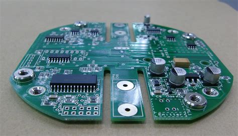
- Consider slotting or barrier creation in the PCB for enhanced isolation
7.2 Reinforced Isolation
- For medical or high-voltage applications, implement additional isolation measures
- Use wider spacing or insulation barriers as required
- Ensure proper transformer construction meets isolation requirements
8. EMI Reduction Techniques
8.1 Input Filter Layout
- Position input filter components close to the power entry point
- Maintain proper grounding for common-mode chokes
- Keep unfiltered and filtered traces separated
8.2 Snubber Circuit Placement
- Place RCD snubber components very close to the MOSFET drain and transformer primary
- Minimize loop area in snubber circuits
- Select appropriate snubber values through testing
8.3 Shielding Considerations
- Use copper pours as local shields for sensitive circuits
- Consider grounded metal shields in high-EMI environments
- Ensure shield grounding doesn’t create ground loops
9. Practical Design Tips
- Layer Stackup: For multilayer boards, dedicate entire layers to ground planes when possible. A 4-layer stack with power-ground-signal-ground is often effective.
- Via Usage: Use multiple vias for high-current paths to reduce impedance and improve thermal performance.
- Test Points: Include accessible test points for critical waveforms (switch node, gate drive, feedback) to facilitate debugging.
- Component Selection: Choose components with PCB layout in mind – some MOSFETs and controllers have optimized pinouts for better layouts.
- Prototyping: Always budget for at least one design iteration to optimize layout based on actual performance measurements.
10. Verification and Testing
After implementing these PCB design techniques, verify the design through:
- Visual Inspection: Check for proper creepage/clearance, trace widths, and component placement
- Continuity Testing: Verify proper connections and absence of shorts
- Power-Up Testing: Gradually bring up voltage while monitoring current draw
- Waveform Analysis: Examine switch node ringing, gate drive quality, and output ripple
- Thermal Imaging: Identify hot spots under full load conditions
- EMI Testing: Conduct pre-compliance testing to identify radiation issues
Conclusion
Effective flyback switch-mode power supply PCB design requires careful attention to component placement, current loop minimization, proper grounding, and thermal considerations. By partitioning the board into functional areas, maintaining tight control over high-frequency switching paths, and implementing robust grounding schemes, designers can achieve efficient, reliable power conversion with minimal EMI. The discontinuous nature of flyback converter operation makes proper layout particularly crucial compared to other topologies. While the principles discussed provide a solid foundation, each design presents unique challenges that may require specific adaptations. Through thoughtful implementation of these guidelines and iterative testing, power supply designers can create compact, efficient flyback converters that meet performance targets while complying with safety and regulatory requirements.

