Key Considerations for Power Plane Design in PCB Layout
Introduction
Power integrity is a critical aspect of printed circuit board (PCB) design, directly impacting the performance, stability, and reliability of electronic systems. A well-designed power distribution network (PDN) ensures stable voltage levels, minimizes noise, and reduces electromagnetic interference (EMI). Among the key elements of PDN design, the power plane plays a vital role in delivering clean and efficient power to integrated circuits (ICs). This article explores the essential considerations for power plane design in PCB layouts, covering material selection, stackup configuration, decoupling strategies, and noise reduction techniques.
1. Power Plane Basics
A power plane is a dedicated copper layer in a PCB that distributes power to various components. Unlike power traces, which have limited current-carrying capacity, power planes provide low-impedance paths, reducing voltage drops and improving power delivery efficiency.
1.1 Power Plane vs. Power Traces
- Power Traces: Suitable for low-current applications but introduce higher resistance and inductance.
- Power Planes: Offer lower impedance, better heat dissipation, and reduced EMI.
1.2 Single vs. Multiple Power Planes
- Single Power Plane: Used in simpler designs with a single voltage rail.
- Multiple Power Planes: Required for complex PCBs with multiple voltage levels (e.g., 3.3V, 5V, 12V).

2. PCB Stackup and Power Plane Placement
The arrangement of power planes in the PCB stackup significantly affects signal integrity and EMI performance.
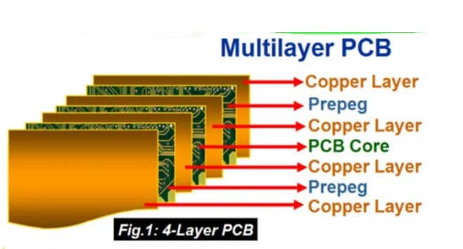
2.1 Optimal Layer Stackup
A typical multilayer PCB stackup includes:
- Signal Layer (Top)
- Ground Plane
- Power Plane
- Signal Layer (Bottom)
Key guidelines:
- Place power and ground planes adjacent to each other to enhance capacitance and reduce noise.
- Avoid placing high-speed signal layers between split power planes to prevent crosstalk.
2.2 Power Plane Splitting
When multiple voltage levels are required, power planes can be split into different regions. Considerations:
- Isolation: Ensure sufficient spacing between different voltage regions to prevent short circuits.
- Return Paths: Maintain a continuous ground plane beneath split power planes to minimize loop inductance.

3. Decoupling and Bypass Capacitors
Decoupling capacitors are essential for stabilizing power supply voltages by filtering high-frequency noise.
3.1 Capacitor Placement
- Place decoupling capacitors as close as possible to IC power pins.
- Use a combination of bulk (10μF–100μF), ceramic (0.1μF), and high-frequency (1nF–10nF) capacitors.
3.2 Power Plane Capacitance
The intrinsic capacitance between power and ground planes helps suppress high-frequency noise. To maximize this effect:
- Use thin dielectric layers (e.g., 4mil FR4) between power and ground planes.
- Ensure low impedance across a wide frequency range.
4. Minimizing Power Noise and EMI
Noise in power planes can lead to signal integrity issues and EMI problems.
4.1 Reducing Ground Bounce
- Use multiple vias to connect power and ground planes, lowering inductance.
- Avoid long, thin power traces that increase resistance.
4.2 EMI Mitigation
- Implement solid power planes instead of gridded designs to reduce radiated emissions.
- Use stitching vias around the edges of power planes to contain electromagnetic fields.

5. Thermal Management
Power planes also act as heat spreaders, helping dissipate heat from high-power components.
5.1 Copper Thickness
- Standard PCBs use 1oz (35μm) copper, but high-current applications may require 2oz or thicker copper.
5.2 Thermal Relief Pads
- Use thermal relief connections for vias and component pads to improve solderability while maintaining thermal conductivity.
6. Simulation and Verification
Before fabrication, power plane integrity should be verified using simulation tools.
6.1 PDN Analysis
- Use tools like Ansys SIwave, Cadence Sigrity, or Keysight ADS to analyze impedance, resonance, and voltage drop.
6.2 Real-World Testing
- Measure power noise with an oscilloscope and perform EMI testing to ensure compliance with standards.
Conclusion
Designing an efficient power plane in a PCB requires careful consideration of stackup, decoupling strategies, noise reduction, and thermal management. By following best practices in power plane layout, engineers can ensure stable power delivery, minimize noise, and enhance the overall reliability of electronic systems. Proper simulation and testing further validate the design, ensuring optimal performance in real-world applications.
By implementing these key principles, PCB designers can achieve robust power integrity, leading to higher-performance and more reliable electronic products.