Key elements affecting PCB manufacturability
As an indispensable part of electronic products, printed circuit boards (PCBs) play a key role in realizing the functions of electronic products, which leads to the increasing importance of PCB design, because the performance of PCB design directly determines the functions and costs of electronic products. Excellent PCB design can keep electronic products away from many problems, ensuring that the products can be manufactured smoothly and can meet all the needs of practical applications.
Among all the elements that contribute to PCB design, design for manufacturing (DFM) is definitely an essential element, because it links PCB design with PCB manufacturing so that problems can be discovered early and solved in time throughout the life cycle of electronic products. A myth is that the complexity of PCB design will increase as the manufacturability of electronic products is considered in the PCB design stage. In the life cycle of electronic product design, DFM can not only enable electronic products to smoothly participate in automated production and save labor costs in the manufacturing process, but also effectively shorten the manufacturing production time to ensure the timely completion of the final electronic products.
PCB Manufacturability
Since manufacturability is combined with PCB design, design for manufacturing is a key element leading to efficient manufacturing, high quality and low cost. The scope of PCB manufacturability research is wide and can generally be divided into PCB manufacturing and PCB assembly.
1. PCB production
In terms of PCB manufacturing, the following aspects should be considered: PCB size, PCB shape, process edge and mark point. Once these aspects are not fully considered in the PCB design stage, the automatic chip mounter may not accept the prefabricated PCB board unless additional processing measures are taken. Worse, some boards cannot participate in automatic manufacturing using manual soldering. As a result, the manufacturing cycle will be extended and the labor cost will increase.
(1)PCB size
Each chip mounter has its own required PCB size, which varies according to the parameters of each mounter. For example, the maximum PCB size accepted by the chip mounter is 500mm450mm, while the minimum PCB size is 30mm30mm. This does not mean that we cannot handle PCB board components smaller than 30mm*30mm, and when a smaller size is required, we can rely on panelization. When only manual installation can be relied on and the labor cost rises and the production cycle is out of control, the chip mounter will never accept PCB boards that are too large or too small. Therefore, in the PCB design stage, the PCB size requirements set by automatic mounting manufacturing must be fully considered and must be controlled within the effective range.
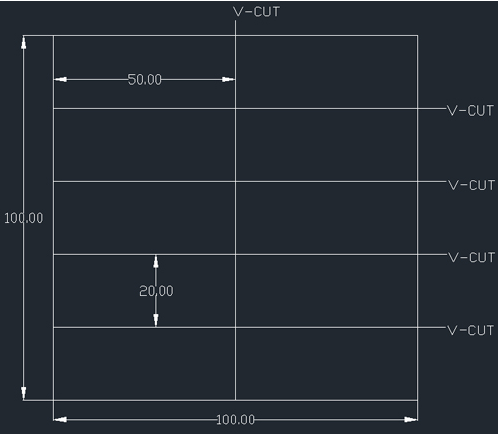
The figure below demonstrates the PCB panel design file completed by the design software. As a 5×2 panel, each square unit is a single board with a size of 50mm20mm. The connection between each unit is achieved by V-cut/V-scoring technology. In this image, the final size of the panel displayed by the entire square is 100mm100mm. According to the above panel size requirements, it can be concluded that the panel size is within the acceptable range.

2.PCB shape
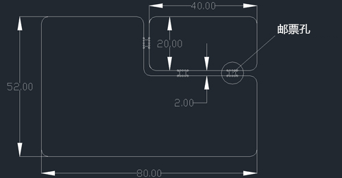
In addition to PCB size, all chip mounters have requirements for PCB shape. The ordinary PCB shape should be rectangular, and its length to width ratio should be 4:3 or 5:4 (optimal). If the shape of the PCB is irregular, additional measures must be taken before SMT assembly, resulting in increased costs. In order to prevent this from happening, the PCB must be designed as a normal shape in the PCB design stage so that it can meet the SMT requirements. However, it is difficult to do this in actual situations. When the shape of some electronic products must be irregular, postholes must be used to make the shape of the final PCB have a normal shape. After assembly, the extra auxiliary baffles can be omitted from the PCB to meet the requirements of automatic installation and space.
The figure below shows an irregularly shaped PCB with a processing edge added by Huaqiu DFM software. The entire circuit board size is 80mm52mm, and the square area is the size of the actual PCB. The size of the upper right corner area is 40mm20mm, which is the auxiliary process edge generated by the posthole bridge.

3.Process edge
In order to meet the needs of automatic manufacturing, a process edge must be placed on the PCB to fix the PCB.
In the PCB design stage, a 5mm wide process edge should be reserved in advance, without any components and traces. The technical rail is usually placed on the short side of the PCB, but the short side can be selected when the aspect ratio exceeds 80%. After assembly, the process edge, which plays an auxiliary production role, can be removed.

4.Reference point (Mark point)
For PCBs with components installed, Mark points should be added as common reference points to ensure that each assembly equipment can accurately determine the component position. Therefore, Mark points are the SMT manufacturing benchmarks required for automatic manufacturing.
Components require 2 Mark points, while PCBs require 3 Mark points. These marks should be placed on the edge of the PCB board and cover all SMT components. The center distance between the Mark point and the edge of the board should be at least 5mm. For PCBs with double-sided SMT components, there should be Mark points on both sides. If the components are placed too densely to place Mark points on the board, they can be placed on the process edge.
PCB assembly
PCB assembly, referred to as PCBA, is actually the process of soldering components on bare boards. In order to meet the requirements of automated manufacturing, PCB assembly has some requirements for component packaging and component layout.
(1)Component packaging
In the PCBA design process, if the component packaging does not meet the appropriate standards and the distance between components is too close, automatic installation will not be performed.
In order to obtain the best component packaging, professional EDA design software should be used to be compatible with international component packaging standards. During the PCB design process, the bird’s-eye view area must not overlap with other areas, and the automatic IC placement machine will be able to accurately identify and perform surface mounting.
(2)Component layout
Component layout is an important task in PCB design because its performance is directly related to the appearance of the PCB and the complexity of the manufacturing process.
During the component layout process, the assembly surface of the SMD component and the THD component should be determined. Here, we set the front side of the PCB as the component A side, and the back side as the component B side. The component layout should consider the assembly form, including single-layer single-package assembly, double-layer single-package assembly, single-layer mixed package assembly, A-side mixed package and B-side single package assembly, and A-side THD and B-side SMD components. Different assemblies require different manufacturing processes and technologies. Therefore, in terms of component layout, the best component layout should be selected to make manufacturing simple and easy, thereby improving the manufacturing efficiency of the entire process.
In addition, the direction of the component layout, the spacing between components, heat dissipation, and component height must be considered.
Generally speaking, the component direction should be consistent. The component layout complies with the principle of the shortest tracking distance, based on which the polarity direction of components with polarity marks should be consistent, while components without polarity marks should be neatly arranged on the X or Y axis. The component height should be a maximum of 4mm, while the transmission direction of the component and PCB should be maintained at 90°.
In order to increase the component soldering speed and facilitate later inspection, the spacing between components should be consistent. Components in the same network should be close to each other, while a safe distance should be left between different networks according to the voltage drop. The silk screen and pads must not overlap, otherwise the components will not be installed.
Due to the actual operating temperature of the PCB and the thermal characteristics of the electrical components, heat dissipation should be considered. The component layout should focus on heat dissipation, and fans or heat sinks should be used when necessary. Appropriate heat sinks should be selected for power components, and heat-sensitive components should be placed away from heat. High components should be placed behind low components.
There are more details that should be focused on PCB DFM, and experience should be accumulated in practice. For example, high-speed signal PCB design requires special requirements for impedance, which should be discussed with the circuit board manufacturer before actual manufacturing to determine the impedance and layering information. In order to prepare for production on some small-sized and densely traced PCB boards, the manufacturing capabilities of the minimum trace width and through-hole diameter should be discussed with the PCB manufacturer to ensure the smooth production of these PCBs.


