Key Points in PCB Design for Flyback Switching Power Supplies
Abstract
The flyback converter is a widely used topology in switching power supply designs due to its simplicity, cost-effectiveness, and ability to provide isolation. However, achieving optimal performance requires careful PCB layout to minimize electromagnetic interference (EMI), reduce power losses, and ensure stable operation. This article discusses the critical PCB design considerations for flyback converters, including grounding strategies, component placement, trace routing, thermal management, and noise suppression techniques.
1. Introduction
Flyback converters are commonly used in low-to-medium power applications such as AC/DC adapters, LED drivers, and auxiliary power supplies. The PCB layout significantly impacts efficiency, EMI performance, and reliability. Poor layout practices can lead to excessive noise, voltage spikes, and even device failure. Therefore, understanding the key PCB design principles is essential for robust flyback converter implementation.
2. Key PCB Design Considerations
2.1 Component Placement
Proper component placement is crucial for minimizing parasitic inductance and resistance, reducing loop areas, and optimizing thermal performance.
- Primary-Side Components:
- Place the input capacitor close to the MOSFET and transformer primary winding to minimize high-frequency current loops.
- Position the PWM controller near the MOSFET gate driver to reduce trace inductance, which can cause switching delays and ringing.
- Secondary-Side Components:
- The output rectifier diode and output capacitor should be placed as close as possible to the transformer’s secondary winding to minimize loop inductance and voltage spikes.
- Transformer Placement:
- The transformer should be positioned to minimize coupling between primary and secondary-side noise.
- Ensure sufficient creepage and clearance distances for safety compliance (e.g., IEC 60950, IEC 62368).
2.2 Grounding Strategy
Grounding is critical in flyback converters to avoid ground loops, noise coupling, and EMI issues.
- Split Ground Planes:
- Use separate ground planes for the primary (high-voltage) and secondary (low-voltage) sides, connected only at a single point near the transformer or optocoupler (if used for feedback).
- Avoid overlapping primary and secondary ground planes to prevent capacitive coupling.
- Star Grounding:
- High-current return paths (e.g., from MOSFET, diode, and input/output capacitors) should converge at a single point to minimize ground bounce.
- Signal Ground vs. Power Ground:
- Keep sensitive analog grounds (e.g., feedback network, control IC) separate from noisy power grounds.
2.3 Trace Routing
Proper trace routing reduces parasitic effects and improves signal integrity.
- High-Current Paths:
- Use wide traces for high-current paths (e.g., primary switch, transformer, output diode) to reduce resistance and inductance.
- Avoid sharp corners; use 45° angles or rounded traces to minimize impedance discontinuities.
- High-Voltage Isolation:
- Maintain adequate spacing between high-voltage traces (e.g., primary-side switching node) and low-voltage traces to prevent arcing and noise coupling.
- Sensitive Signal Traces:
- Route feedback and control signals away from high-frequency switching nodes to avoid noise pickup.
- Use guard traces or ground shielding for critical analog signals.
2.4 Minimizing EMI and Noise
Flyback converters generate significant EMI due to high-frequency switching. Proper PCB design can mitigate these effects.
- Snubber Circuits:
- Place snubber components (resistor, capacitor, diode) close to the MOSFET or rectifier diode to suppress voltage spikes.
- Shielding and Filtering:
- Use ferrite beads or common-mode chokes on input/output lines to suppress conducted EMI.
- Implement a ground plane beneath high-frequency switching nodes to reduce radiated emissions.
- Loop Area Minimization:
- Keep high di/dt loops (e.g., primary switch-transformer-input capacitor) as small as possible to reduce magnetic field radiation.
2.5 Thermal Management
Power dissipation in flyback converters can lead to overheating if not properly managed.
- Copper Pour and Heatsinking:
- Use large copper areas for power components (MOSFET, diode) to improve heat dissipation.
- Add thermal vias under hot components to transfer heat to inner layers or the bottom side.
- Component Spacing:
- Ensure adequate airflow around heat-generating components (e.g., transformer, MOSFET).
2.6 Safety and Compliance
Flyback converters must meet safety standards for isolation and creepage/clearance.
- Isolation Barriers:
- Maintain proper creepage (distance along the surface) and clearance (air gap) between primary and secondary sides.
- Use slots or cutouts in the PCB to increase isolation distances if necessary.
- Reinforced Insulation (for High-Voltage Designs):
- Follow standards such as IEC 60950 or IEC 62368 for reinforced insulation requirements.
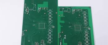
3. Practical PCB Layout Example
A well-designed flyback PCB layout should:
- Place input capacitors near the MOSFET and transformer.
- Keep high-current loops tight and minimize trace inductance.
- Separate primary and secondary grounds while maintaining a single connection point.
- Route feedback signals away from noisy switching traces.
- Implement proper EMI filtering and shielding techniques.
4. Conclusion
The PCB layout of a flyback switching power supply significantly impacts its performance, efficiency, and reliability. By following best practices in component placement, grounding, trace routing, EMI suppression, and thermal management, designers can achieve a robust and high-performance flyback converter. Careful attention to safety standards and noise reduction techniques ensures compliance and long-term reliability in real-world applications.


