Key points of PCB layout design in DCDC chip
I have written several articles about Buck and Boost, but PCB layout is rarely mentioned. This article will talk about PCB layout.
Many manuals of DCDC chips have corresponding PCB layout design requirements, and some also provide some layout schematics, which are similar.
For example, I will list a few key points of buck design:
- The input capacitor and diode are on the same surface as the IC, as close to the IC as possible.
- The inductor is close to the SW of the chip, and the output capacitor is placed close to the inductor.
- The feedback loop is away from noise sources such as inductor, SW and diode.
Do you know where these key points come from?
If you get a specific chip, these conditions may not be met at the same time due to the problem of chip pin distribution, what should you do? Which is more important?
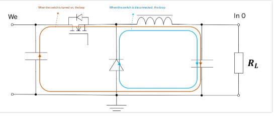
Take Buck as an example
For example, the pin distribution of the buck below is not good.
SW is between IN and GND. If we follow the key points and directly place the input filter capacitor next to IN and GND, the SW signal will not come out, and the inductor is also required to be placed next to the chip, which is a contradiction.
The layout recommended by the chip manual is placed nearby, but its method is to route SW under the input filter capacitor. Are you kidding me? Can this be done in reality?
We cannot use the method recommended by the chip manual, but the fact is that there are many chips with this pin distribution, so how should our layout be laid out and wired?
I will not answer this question first, I will tell you the most fundamental method:
The ultimate secret of DCDC Layout – have a loop in mind
Have a loop in mind
“Loop” refers to a closed loop with a large current flowing through. As long as we control this loop, the layout is basically half successful.
Let’s see why
Take BUCK as an example. The BUCK circuit has two states, the upper tube is turned on and the lower tube (or diode) is turned on, so there are two large current loops.
What is the use of knowing these two loops?
We want to make the area of these two loops as small as possible, because each current loop can be regarded as a loop antenna, which will generate radiation, cause EMI problems, and interfere with other circuits on the board, and the size of the radiation is proportional to the area of the loop.
The high-frequency magnetic field generated by the current loop will gradually convert into an electromagnetic field after leaving the loop for about 0.16λ, and the resulting field strength is approximately:
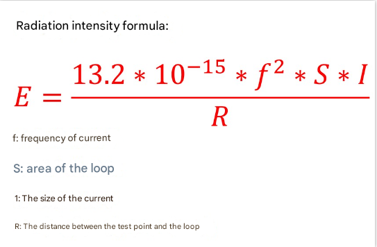
It can be seen that the size of the radiation is proportional to the area of the loop, the square of the frequency, and the size of the current.
So can we just minimize the area of these two loops?
Indeed, but I think it is not enough to understand this point, and it cannot highlight the key points.
As can be seen from the topology diagram, the two loops have a common part, and one loop contains another loop, which causes the current of the large loop to be different at each device node, so it is not easy to calculate using that formula.
So, we need to make some adjustments. How can we make some adjustments?
The reason for radiation is that the current generates a magnetic field. The current is changing, so the magnetic field is also changing. The magnetic flux in the area surrounded by the current loop will change with the dynamic change of the current. The magnetic field generates an electric field, and the electric field generates a magnetic field to form an electromagnetic wave.
We disassemble the large current loop into two parts, as shown below:
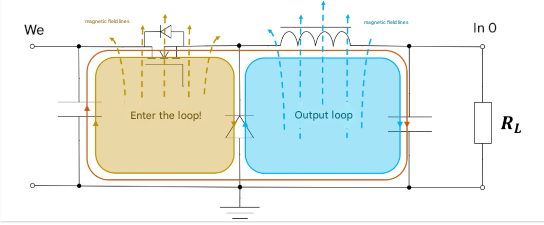
The entire large loop can be seen as a superposition of the input loop and the output loop.
It may be a bit difficult to understand, because the input loop is not an actual current loop at all, it is the difference between the two existing current loops.
This is actually just an equivalent method. Our goal is to know the change of magnetic flux in the total large loop, so that we can calculate it after equivalent. We can calculate the magnetic flux of the input loop and the output loop respectively.
The equivalent current of the input loop is the current of the input capacitor Cin
The circuit equivalent current of the output loop is the current of the inductor
They only look at the AC component, regardless of the DC component. The frequency of DC is considered to be 0Hz, and no electromagnetic waves will be radiated.
Previously, our “Buck Tear! Buck Formula Derivation Process” has been analyzed. The input loop current (Cin) and the output loop current (inductor) are as follows:
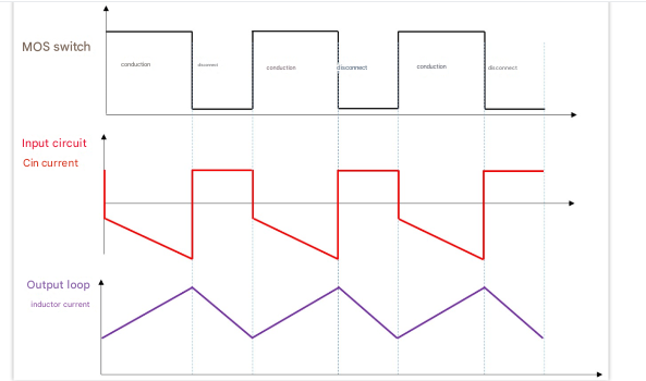
It can be seen that when the switch is switched, the current of the input loop will change suddenly, that is, there will be a large di/dt, then the magnetic flux of the input loop will also change suddenly (to be precise, the change speed is very fast), and there are many high-order harmonics.
From the previous formula, we know that the radiation intensity is proportional to the frequency, so these high-order harmonics are more likely to be radiated.
The current of the output loop is a triangular wave, which has no mutations, so the radiation intensity of the high-order harmonics is smaller.
Signal strength comparison
Some people may say here, isn’t the spectrum of the triangular wave theoretically infinite? There are also many high-frequency components, so how can the radiation be smaller?
Indeed, the spectrum of the triangular wave is infinite, but the higher the frequency, the lower the amplitude, that is, the less energy the high-frequency component has, so the radiation is also less.
Regarding this point, we simply do a simulation and look at the Fourier transform fft of the current to know.
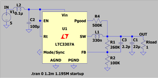
Using LTspice software simulation, the 5V to 1.8V buck circuit diagram is as follows:
Input loop current (input capacitor current) and output loop current (inductor current waveform)
With the waveform, let’s look at fft (simulation software can easily do it)
You can see that the base frequency is the switching frequency of the BUCK chip LTC3307A, 2Mhz. The difference in strength between the two at 2Mhz is not very large, only about 2-3db, but at 10Mhz, the difference is already 20db. The higher the frequency, the greater the difference.
In other words, the high-frequency harmonic energy of the input loop is much greater than that of the output loop. If you have experience, you should know that the high-frequency excess that causes EMI is generally caused by excessive EMI, so the possibility of EMI caused by the input loop is higher.
I spent some effort here, actually just to explain:
The input loop of the BUCK is very, very important, and the loop area must be small.
Another point to note is that the loop area is small, not the line is short. There is a difference between the two. Sometimes a short line does not necessarily mean a small loop. Our goal is the area of the loop, not the length.
We try to make the layout of the line flat.
Let’s go back to the DCDC chip at the beginning. What does the input loop refer to?
Obviously, the switch tube of this chip is inside the chip, so the input loop is the loop formed by the chip’s IN pin, the GND pin, and the input filter capacitor. Then, in addition to the chip, the device only has the input filter capacitor.
Therefore, the most ideal layout is to directly connect the input filter capacitor to the chip’s IN pin and GND pin. From this point of view, the layout recommended by the chip manual is consistent with this point, but after doing this, the SW cannot come out.
The recommended layout given by this DCDC chip does ensure that the input loop is minimized. It’s just that it routes the SW signal under the input filter capacitor. This actual circuit is usually not feasible because a wider line cannot be routed under the capacitor.
What should we do?
I guess some people think that placing the input filter capacitor on the back of the PCB, placing the filter capacitor directly below the Vin and GND pins, and connecting them through vias will make the loop look smaller.
My opinion is that if there are other better ways, don’t do it.
Because vias will have parasitic inductance, adding vias will increase the inductance of the loop, resulting in LC oscillation. The direct phenomenon is high ringing at SW, which means that the signal component of the resonant frequency in this loop is very strong.
In other words, although the loop area is not large and the antenna effect is not strong, my signal strength has increased, and the radiation is not necessarily bad.
Regarding ringing, I have written a special article “Buck’s Ringing Experiment and Analysis” before, you can go and have a look.
Previous lessons
Many years ago, I encountered a power chip input filter capacitor placed on the back and connected through vias, which made the whole board very noisy. However, if the filter capacitor was manually connected directly to Vin and GND, the problem would be solved immediately.
At that time, I didn’t understand it and found it incredible. There were quite a few holes, and the filter capacitor was placed near the bottom. There was still a problem. How could a few holes have such a big impact?
Later, I specially modified the board to solve it. I directly placed the input filter capacitor on the same layer as the chip and connected it on the surface. The problem was solved.
I have said so much above, but the main point is that the layout and wiring of the input filter capacitor in the BUCK circuit is very important. It is the top priority and the first thing to consider.
If it is an asynchronous Buck, then there is an external diode. This diode constitutes part of the input loop. Then its position is at the same level of importance as the input filter capacitor. It should be placed close to the SW of the chip. How to place it specifically can be seen from how small the loop area is.
Output loop
I have written a lot before, and I have been emphasizing the input loop. Is the output loop not important?
Of course not. In fact, from the previous fft, we can see that the output loop also has high-frequency components, so the output loop should be as small as possible. However, the high-frequency component intensity is not high compared to the input loop. When there is a conflict between the two layouts, the input loop is of course given priority.
How do I draw it?
In short, if it were me, I would lay out the BUCK mentioned at the beginning like this:
What about boost?
The above is a case of buck, so what about boost?
Is the input loop the most important? Is the input filter capacitor the first thing to consider?
The answer is NO
Boost also has two loops, as shown in the figure below
Like buck, we divide them into two parts, the input loop and the output loop. It can be seen that the output loop is the difference between the above two loops.
Unlike buck, the inductor is in the input loop, and its current waveform is a three-legged wave, while the current in the output loop is the current of the diode, which has a sudden change.
Previously, “Tear Boost! The Boost Formula Derivation and Experimental Verification has also comprehensively analyzed these two currents, and the waveforms are as follows:
That is to say, the most important thing about boost is the output loop, which is similar to the input loop of Buck. What we need to ensure first is that the output loop of boost is as small as possible.
Specific examples will not be given.
Other considerations for layout
In addition to the large current loop, there are FB and compensation circuits, which are small signal circuits, so they should be kept as far away from the large current loop in front as possible, away from inductors, etc.
For example, the following is better on the left than on the right:
In addition, it should be noted that for large current loops, we should consider the GND ground, and do not use these traces to divide the GND path of the return ground of the large current.
Therefore, sometimes you will see that the bottom FB trace is not the shortest, but it is around.
Summary
In general, for the layout of DCDC, we must have the current loop in mind.
When drawing the board, think about it in your mind, when the switch is turned off, the current flows, when the switch is turned on, the current flows. Then find the loop where the current suddenly changes, which is the most important and should be handled first.
This principle is not only applicable to DCDC, but also to other types of power supplies or high-power circuits.
Knowing this principle, in fact, for many circuits, there is no need to look closely at the precautions for PCB layout in the chip manual. It just talks about these things, but they are just specific measures.
This method of minimizing the critical loop is to eliminate the problem from the root, which is much better than not changing the board at a later stage and then messing around.