Kicad pcb assembly
Introduction To KiCad PCB Assembly: A Beginner’s Guide
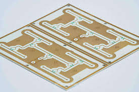
KiCad PCB assembly is an essential process in the realm of electronics design and manufacturing, offering a comprehensive suite of tools for creating printed circuit boards (PCBs). As an open-source software, KiCad has gained significant popularity among hobbyists, educators, and professionals alike, due to its robust features and cost-effectiveness. Understanding the basics of KiCad PCB assembly is crucial for anyone looking to delve into the world of electronics design, as it provides the foundation for creating functional and efficient electronic devices.
To begin with, KiCad is a powerful electronic design automation (EDA) tool that facilitates the design and layout of PCBs.
It encompasses a range of features, including schematic capture, PCB layout, and a 3D viewer, which collectively streamline the process of designing electronic circuits. The software’s user-friendly interface and extensive library of components make it accessible to beginners, while its advanced capabilities cater to the needs of experienced designers. As a result, KiCad serves as an ideal platform for learning and mastering the intricacies of PCB assembly.
Transitioning from the design phase to the assembly phase involves several critical steps.
Initially, the designer must create a schematic diagram, which serves as a blueprint for the electronic circuit. This diagram outlines the connections between various components, such as resistors, capacitors, and integrated circuits, and is essential for ensuring the circuit’s functionality. KiCad’s schematic editor provides a range of tools for drawing and annotating schematics, allowing designers to accurately represent their circuits.
Once the schematic is complete, the next step is to transfer the design to the PCB layout editor.
This phase involves arranging the components on the board and routing the electrical connections between them. KiCad’s layout editor offers a variety of features to assist in this process, including automatic routing, design rule checks, and a 3D viewer to visualize the final product. These tools help designers optimize the layout for performance and manufacturability, ensuring that the PCB meets the desired specifications.
After finalizing the PCB layout, the designer must generate the necessary files for manufacturing.
KiCad simplifies this process by providing options to export Gerber files, which are the standard format used by PCB manufacturers. These files contain detailed information about the board’s layers, including copper traces, solder masks, and silkscreens, and are crucial for the fabrication of the PCB. Additionally, KiCad allows designers to create a bill of materials (BOM), which lists all the components required for assembly, further streamlining the manufacturing process.
In conclusion, KiCad PCB assembly is a vital skill for anyone interested in electronics design, offering a comprehensive and accessible platform for creating PCBs. By understanding the key steps involved in the process, from schematic capture to layout design and file generation, beginners can effectively harness the power of KiCad to bring their electronic projects to life. As technology continues to advance, the demand for skilled PCB designers will only grow, making KiCad an invaluable tool for aspiring engineers and hobbyists alike. Through practice and exploration, users can unlock the full potential of KiCad, paving the way for innovative and efficient electronic designs.

Advanced Techniques In KiCad For Efficient PCB Assembly
KiCad, an open-source software suite for electronic design automation, has become increasingly popular among engineers and hobbyists for designing printed circuit boards (PCBs). As the complexity of electronic devices grows, so does the need for efficient PCB assembly techniques. Advanced techniques in KiCad can significantly enhance the efficiency and accuracy of PCB assembly, ensuring that the final product meets the desired specifications and performance standards.
One of the fundamental aspects of efficient PCB assembly in KiCad is the strategic placement of components.
Proper component placement not only affects the functionality of the circuit but also impacts the ease of assembly and the overall reliability of the PCB. By utilizing KiCad’s interactive placement tools, designers can optimize the layout to minimize trace lengths and reduce electromagnetic interference. This is particularly important in high-frequency circuits where signal integrity is paramount. Moreover, KiCad allows for the creation of custom component footprints, enabling designers to tailor the layout to specific assembly requirements and constraints.
Transitioning from component placement to routing, KiCad offers advanced routing capabilities that facilitate efficient PCB assembly.
The software’s push-and-shove router is a powerful tool that allows designers to route complex boards with ease. This feature enables the automatic adjustment of traces to accommodate new routes, thereby optimizing the use of available space on the PCB. Additionally, KiCad supports differential pair routing, which is essential for maintaining signal integrity in high-speed digital circuits. By ensuring that differential pairs are routed with consistent spacing and length, designers can prevent signal degradation and improve the overall performance of the PCB.
Another advanced technique in KiCad for efficient PCB assembly is the use of design rule checks (DRCs).
DRCs are essential for verifying that the PCB design adheres to manufacturing constraints and industry standards. KiCad’s DRC feature allows designers to define custom rules that reflect the specific requirements of their project. By running DRCs throughout the design process, potential issues can be identified and addressed early, reducing the likelihood of costly errors during assembly. Furthermore, KiCad’s electrical rule check (ERC) complements DRCs by ensuring that the schematic design is electrically sound, thus preventing functional issues in the final product.
In addition to these techniques, KiCad’s integration with external tools and libraries can further enhance the efficiency of PCB assembly.
For instance, KiCad can interface with simulation software to validate circuit behavior before physical assembly. This integration allows designers to identify and rectify potential issues in the virtual environment, saving time and resources. Moreover, KiCad’s extensive library of components and footprints, along with its support for third-party libraries, provides designers with a vast array of options for sourcing components that meet their specific needs.
Finally, documentation is a critical component of efficient PCB assembly, and KiCad excels in this area by providing comprehensive tools for generating assembly drawings and bills of materials (BOMs).
These documents are essential for communicating design intent to manufacturers and ensuring that the assembly process proceeds smoothly. By leveraging KiCad’s documentation capabilities, designers can produce detailed and accurate documentation that facilitates efficient and error-free assembly.
In conclusion, advanced techniques in KiCad play a crucial role in enhancing the efficiency of PCB assembly. Through strategic component placement, advanced routing capabilities, rigorous design rule checks, integration with external tools, and comprehensive documentation, KiCad empowers designers to create high-quality PCBs that meet the demands of modern electronic devices. As technology continues to evolve, mastering these techniques will be essential for staying competitive in the field of electronic design.
Common Challenges In KiCad PCB Assembly And How To Overcome Them
KiCad, an open-source software suite for electronic design automation, has become increasingly popular among engineers and hobbyists for designing printed circuit boards (PCBs). However, despite its robust features and user-friendly interface, users often encounter several challenges during the PCB assembly process. Understanding these common issues and learning how to effectively address them can significantly enhance the efficiency and success of your projects.
One of the primary challenges in KiCad PCB assembly is managing component libraries.
KiCad offers a vast array of components, but the default libraries may not always include the specific parts needed for a project. This can lead to difficulties in sourcing components and ensuring their compatibility with the design. To overcome this, users can create custom libraries or import third-party libraries that contain the necessary components. By doing so, designers can ensure that all required parts are readily available, thus streamlining the assembly process.
Another frequent issue is the accurate placement of components on the PCB layout. Misplaced components can lead to design errors and functional failures.
To mitigate this risk, it is crucial to utilize KiCad’s design rule checks (DRC) and electrical rule checks (ERC) features. These tools help identify potential errors in the design, such as incorrect trace widths or spacing violations, before the board is manufactured. Additionally, using the 3D viewer in KiCad can provide a visual representation of the board, allowing designers to verify component placement and orientation.
Signal integrity is another critical aspect that can pose challenges during PCB assembly.
Poor signal integrity can result in electromagnetic interference (EMI) and signal degradation, affecting the overall performance of the circuit. To address this, designers should pay close attention to trace routing, ensuring that high-speed signals are routed with minimal length and avoiding sharp angles. Implementing proper grounding techniques and using decoupling capacitors can also help maintain signal integrity.
Thermal management is a further consideration that can complicate the assembly process.
Components that generate significant heat can lead to thermal issues, potentially damaging the board or affecting its performance. To combat this, designers should incorporate thermal vias and heat sinks into their designs. Additionally, conducting thermal simulations using KiCad’s integrated tools can help identify potential hotspots and allow for adjustments before the board is fabricated.
Moreover, documentation and version control are often overlooked but are essential components of successful PCB assembly.
Inadequate documentation can lead to assembly errors and miscommunication among team members. To prevent this, designers should maintain comprehensive documentation, including schematics, bill of materials (BOM), and assembly instructions. Utilizing version control systems can also help track changes and ensure that all team members are working with the most up-to-date design files.
In conclusion, while KiCad offers a powerful platform for PCB design, users may encounter several challenges during the assembly process.
By proactively addressing issues related to component libraries, component placement, signal integrity, thermal management, and documentation, designers can enhance the reliability and performance of their PCBs. Employing these strategies not only improves the assembly process but also contributes to the overall success of electronic projects. As KiCad continues to evolve, staying informed about best practices and leveraging its features will be key to overcoming these common challenges.

Optimizing Your KiCad Workflow For Faster PCB Assembly
Optimizing your KiCad workflow for faster PCB assembly is an essential step in enhancing productivity and ensuring the timely completion of electronic projects. As the demand for rapid prototyping and efficient production processes increases, leveraging the capabilities of KiCad, an open-source electronic design automation (EDA) tool, becomes crucial. By streamlining your workflow, you can significantly reduce the time and effort required to transition from design to assembly, thereby accelerating the overall development cycle.
To begin with, understanding the importance of a well-organized component library cannot be overstated.
A comprehensive and meticulously maintained library serves as the foundation for efficient design processes. By categorizing components logically and ensuring that each part is accurately defined with all necessary parameters, you can minimize errors and avoid unnecessary delays during the design phase. Moreover, utilizing KiCad’s library management features, such as symbol and footprint editors, allows for the customization and standardization of components, which further enhances the consistency and reliability of your designs.
In addition to a robust component library, adopting a systematic approach to schematic design is vital.
This involves creating clear and concise schematics that are easy to interpret and modify. By adhering to best practices, such as using hierarchical sheets and consistent naming conventions, you can simplify the design process and facilitate collaboration among team members. Furthermore, taking advantage of KiCad’s electrical rules check (ERC) feature helps identify potential issues early in the design phase, thereby reducing the likelihood of errors propagating to the assembly stage.
Transitioning from schematic to layout is another critical step where optimization can yield significant time savings.
KiCad’s layout editor offers a range of tools to streamline this process, including automatic routing and design rule checks (DRC). By configuring these tools to align with your specific design requirements, you can expedite the layout process while ensuring compliance with industry standards. Additionally, employing techniques such as component placement optimization and efficient trace routing can further enhance the manufacturability of your PCB, ultimately leading to faster assembly times.
Moreover, generating accurate and comprehensive fabrication outputs is essential for seamless communication with manufacturers.
KiCad provides a variety of export options, including Gerber files, drill files, and bill of materials (BOM), which are crucial for the assembly process. Ensuring that these outputs are meticulously reviewed and verified before submission can prevent costly errors and rework. Furthermore, collaborating closely with your manufacturer to understand their specific requirements and capabilities can facilitate smoother transitions from design to production.
Finally, continuous learning and adaptation are key to maintaining an optimized KiCad workflow.
As technology evolves and new features are introduced, staying informed about the latest updates and best practices can provide a competitive edge. Engaging with the KiCad community through forums, tutorials, and workshops can offer valuable insights and foster a culture of continuous improvement. By embracing these opportunities for growth, you can refine your workflow and achieve faster, more efficient PCB assembly.
In conclusion, optimizing your KiCad workflow for faster PCB assembly involves a multifaceted approach that encompasses library management, schematic design, layout optimization, and effective communication with manufacturers. By implementing these strategies and remaining adaptable to technological advancements, you can enhance your productivity and ensure the successful completion of your electronic projects.


