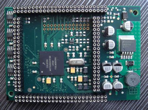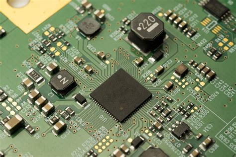
Klicky pcb assembly
Understanding The Klicky PCB Assembly Process: A Step-by-Step Guide
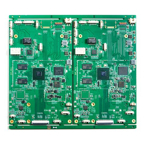
The process of Klicky PCB assembly is a meticulous and intricate procedure that requires precision and attention to detail. Understanding this process is essential for anyone involved in electronics manufacturing or design. The assembly of printed circuit boards (PCBs) is a critical step in the production of electronic devices, as it involves the integration of various electronic components onto a single board to create a functional circuit. This guide aims to provide a comprehensive overview of the Klicky PCB assembly process, elucidating each step to offer a clearer understanding of how these essential components are brought together.
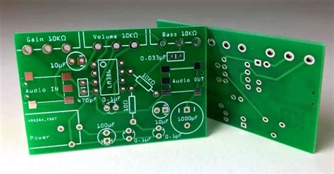
Initially, the process begins with the design and preparation of the PCB layout.
This involves using specialized software to create a schematic diagram that outlines the electrical connections and component placements on the board. Once the design is finalized, it is converted into a format suitable for manufacturing, typically a Gerber file. This file serves as a blueprint for the PCB fabrication, detailing the precise locations for drilling holes, cutting traces, and placing components.
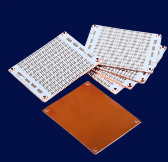
Following the design phase, the next step is the fabrication of the PCB itself.
This involves creating the physical board from a substrate material, usually fiberglass, coated with a thin layer of copper. The copper is etched away to form the circuit traces, which are the pathways that connect different components. This stage also includes drilling holes for through-hole components and vias, which are used to connect different layers of the board.
Once the PCB is fabricated, the assembly process can commence. This begins with the application of solder paste to the board.
Solder paste is a mixture of tiny solder balls and flux, which helps the solder adhere to the board and components. The paste is applied using a stencil that ensures it is placed only on the pads where components will be mounted. This step is crucial, as it ensures that the components are securely attached to the board.
After the solder paste application, the components are placed onto the board.
This is typically done using automated machines that can accurately position thousands of components per hour. These machines use a pick-and-place method, where components are picked up from reels or trays and placed onto the board with precision. The accuracy of this step is vital, as even a slight misalignment can lead to circuit failure.
Following component placement, the board undergoes a reflow soldering process.
During this stage, the board is passed through an oven where it is gradually heated to melt the solder paste. As the solder cools, it solidifies, forming a strong electrical and mechanical bond between the components and the board. This step is critical for ensuring the reliability and functionality of the final product.
Finally, the assembled PCB is subjected to a series of inspections and tests to verify its quality and performance.
Visual inspections are conducted to check for any obvious defects, such as misaligned components or solder bridges. More advanced testing methods, such as automated optical inspection (AOI) and X-ray inspection, are used to detect hidden defects. Functional testing is also performed to ensure that the board operates as intended.
In conclusion, the Klicky PCB assembly process is a complex and detailed procedure that requires careful planning and execution. Each step, from design to testing, plays a crucial role in ensuring the production of high-quality electronic devices. Understanding this process is essential for anyone involved in the electronics industry, as it provides the foundation for creating reliable and efficient products.
Benefits Of Using Klicky PCB Assembly For Your Electronics Projects
Klicky PCB assembly has emerged as a significant advancement in the field of electronics, offering numerous benefits for both hobbyists and professionals engaged in electronics projects. This innovative approach to printed circuit board assembly streamlines the process, enhancing efficiency and precision. One of the primary advantages of using Klicky PCB assembly is its ability to significantly reduce the time required for assembling electronic components. Traditional methods often involve manual soldering, which can be time-consuming and prone to human error. In contrast, Klicky PCB assembly utilizes automated processes that ensure components are placed accurately and securely, thereby minimizing the risk of defects and rework.
Moreover, the precision offered by Klicky PCB assembly is unparalleled.
The automated systems employed in this method are capable of handling even the most intricate designs with remarkable accuracy. This precision is particularly beneficial for complex projects that require the integration of numerous small components. By ensuring that each component is placed correctly, Klicky PCB assembly enhances the overall reliability and performance of the final product. Additionally, this level of accuracy reduces the likelihood of short circuits and other issues that can arise from improper component placement, thereby extending the lifespan of the electronic device.
Another notable benefit of Klicky PCB assembly is its cost-effectiveness.
While the initial investment in automated assembly equipment may be higher than traditional methods, the long-term savings are substantial. The reduction in labor costs, coupled with the decrease in material waste due to fewer errors, results in a more economical production process. Furthermore, the speed and efficiency of Klicky PCB assembly allow for faster turnaround times, enabling manufacturers to meet tight deadlines and respond swiftly to market demands. This agility is crucial in the fast-paced world of electronics, where staying ahead of the competition is essential.
In addition to these practical advantages, Klicky PCB assembly also supports greater design flexibility.
The technology accommodates a wide range of component types and sizes, allowing designers to experiment with innovative layouts and configurations. This flexibility is particularly advantageous for projects that require custom solutions or unique design elements. By facilitating creative freedom, Klicky PCB assembly empowers engineers and designers to push the boundaries of what is possible in electronic design.
Furthermore, the environmental benefits of Klicky PCB assembly should not be overlooked.
The precision and efficiency of the process result in less material waste, contributing to more sustainable manufacturing practices. As the electronics industry continues to grapple with the challenges of e-waste and resource conservation, adopting methods that minimize environmental impact is increasingly important. Klicky PCB assembly aligns with these goals by promoting responsible production practices.
In conclusion, Klicky PCB assembly offers a multitude of benefits that make it an attractive option for electronics projects. Its ability to enhance efficiency, precision, and cost-effectiveness, coupled with its support for design flexibility and environmental sustainability, positions it as a valuable tool for both hobbyists and professionals. As technology continues to evolve, embracing innovative solutions like Klicky PCB assembly will be crucial for those seeking to remain competitive and forward-thinking in the ever-changing landscape of electronics.
Common Challenges In Klicky PCB Assembly And How To Overcome Them
Klicky PCB assembly, a crucial process in the manufacturing of electronic devices, involves the precise placement and soldering of components onto a printed circuit board (PCB). Despite advancements in technology, this process is not without its challenges. Understanding these common issues and implementing effective solutions is essential for ensuring the reliability and functionality of the final product.
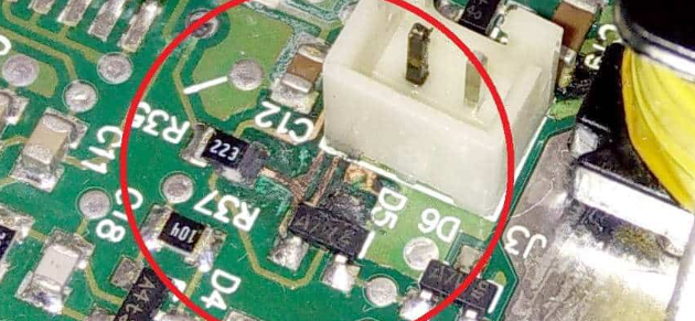
One of the primary challenges in klicky PCB assembly is component misalignment.
This issue often arises due to inaccuracies in the placement of components, which can lead to poor electrical connections and, ultimately, device failure. To overcome this, manufacturers can employ automated optical inspection (AOI) systems. These systems use high-resolution cameras to detect misalignments and other defects early in the assembly process, allowing for timely corrections. Additionally, investing in high-precision pick-and-place machines can significantly reduce the likelihood of misalignment by ensuring components are accurately positioned on the PCB.
Another prevalent challenge is soldering defects, which can manifest as solder bridges, cold joints, or insufficient solder.
These defects can compromise the electrical integrity of the circuit, leading to intermittent connections or complete failure. To address soldering issues, manufacturers should focus on optimizing the reflow soldering process. This involves carefully controlling the temperature profile to ensure that solder paste melts and solidifies correctly, forming strong, reliable joints. Regular maintenance and calibration of soldering equipment are also crucial to prevent defects caused by equipment wear and tear.
Thermal management is another critical aspect of klicky PCB assembly that can pose significant challenges.
As electronic devices become more compact and powerful, managing heat dissipation becomes increasingly important to prevent overheating and ensure longevity. To tackle this issue, designers can incorporate thermal vias, heat sinks, and thermal interface materials into the PCB design. These elements help to efficiently dissipate heat away from critical components, maintaining optimal operating temperatures. Additionally, conducting thorough thermal simulations during the design phase can help identify potential hotspots and allow for proactive design adjustments.
Component availability and supply chain disruptions also present challenges in klicky PCB assembly.
The global electronics industry is highly susceptible to fluctuations in component availability, which can lead to production delays and increased costs. To mitigate these risks, manufacturers should establish strong relationships with multiple suppliers and maintain a strategic inventory of critical components. Implementing a robust supply chain management system can also enhance visibility and enable proactive responses to potential disruptions.
Finally, ensuring compliance with industry standards and regulations is a challenge that cannot be overlooked.
Non-compliance can result in costly recalls and damage to a company’s reputation. To ensure adherence to relevant standards, manufacturers should implement comprehensive quality control processes throughout the assembly process. This includes regular audits, employee training, and staying informed about changes in regulations.
In conclusion, while klicky PCB assembly presents several challenges, understanding these issues and implementing effective solutions can significantly enhance the quality and reliability of electronic devices. By leveraging advanced technologies, optimizing processes, and maintaining a proactive approach to supply chain management and compliance, manufacturers can overcome these challenges and achieve successful PCB assembly.
Innovations In Klicky PCB Assembly: What To Expect In The Future
Klicky PCB assembly, a pivotal process in the electronics manufacturing industry, has witnessed significant advancements over the years. As technology continues to evolve, the future of klicky PCB assembly promises even more innovative developments that are set to revolutionize the industry. Understanding these potential advancements requires a closer look at the current trends and the direction in which the industry is heading.
To begin with, automation is playing an increasingly crucial role in klicky PCB assembly.
The integration of robotics and artificial intelligence into the assembly process has already begun to streamline operations, reduce human error, and increase production efficiency. In the future, we can expect even more sophisticated automation technologies to emerge. These advancements will likely include enhanced machine learning algorithms that can predict and rectify potential assembly issues before they occur, thereby minimizing downtime and improving overall product quality.
Moreover, the miniaturization of electronic components continues to challenge traditional assembly methods.
As devices become smaller and more complex, the demand for precision in PCB assembly grows. Future innovations are likely to focus on developing new techniques and equipment capable of handling these minute components with greater accuracy. For instance, advancements in 3D printing technology could play a significant role in this area, allowing for the creation of intricate circuit designs that were previously impossible to achieve with conventional methods.
In addition to automation and miniaturization, sustainability is becoming an increasingly important consideration in klicky PCB assembly.
As environmental concerns rise, the industry is under pressure to adopt more eco-friendly practices. This shift is expected to drive the development of new materials and processes that reduce waste and energy consumption. For example, the use of biodegradable substrates and lead-free soldering techniques are likely to become more prevalent, aligning with global efforts to minimize the environmental impact of electronic manufacturing.
Furthermore, the Internet of Things (IoT) is set to have a profound impact on klicky PCB assembly.
As more devices become interconnected, the demand for PCBs that can support IoT applications is expected to surge. This will necessitate the development of PCBs with enhanced connectivity and data processing capabilities. In response, manufacturers are likely to invest in research and development to create PCBs that can seamlessly integrate with IoT networks, ensuring reliable performance and data security.
Another area of potential innovation lies in the realm of flexible and wearable electronics.
As consumer demand for wearable technology grows, so too does the need for flexible PCBs that can conform to various shapes and surfaces. Future advancements in materials science are expected to yield new substrates and conductive inks that enable the production of highly flexible and durable PCBs. This will open up new possibilities for the design and functionality of wearable devices, further expanding the applications of klicky PCB assembly.
In conclusion, the future of klicky PCB assembly is poised for exciting developments driven by automation, miniaturization, sustainability, IoT integration, and flexible electronics. As these innovations continue to unfold, they will not only enhance the efficiency and capabilities of PCB assembly but also pave the way for new applications and opportunities in the electronics industry. By staying abreast of these trends, manufacturers can position themselves at the forefront of this rapidly evolving field, ensuring their competitiveness in an increasingly dynamic market.