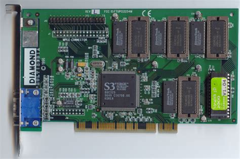
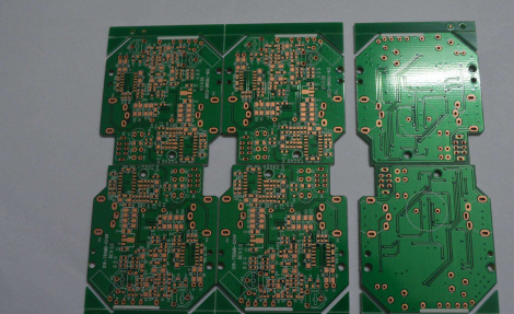
LED display unit board PCB design rules
1.General rules
(1) When the design rules are met, the production cost should be reduced as much as possible, such as: if a 2-layer board can be used, try to use a 2-layer board; when the cost and design rules conflict, ensure the design rules.
(2) The components are arranged neatly, and the same chips are arranged in rows and columns according to certain rules; the spacing between components should take into account the production process and should not affect welding.
(3) For PCB design, automatic wiring cannot be used for design.
2.Details
(1) Use of wiring layer
When designing circuit boards with more than 2 layers, it is prohibited to use the inner electrical layer. Define the inner layer and use it the same as the ordinary layer.
For unit boards that require blind and buried hole design, for four-layer boards, 1-2, 3-4, 1-4 are punched; for six-layer boards, 1-2, 2-5, 5-6 are punched; the specific process must be confirmed with the PCB manufacturer.
(2) Separate power supply for digital devices and driver devices
The digital ground and analog ground should be separated by wiring. The power supply of the digital part is only connected to the power supply of the driver part through a jumper at the entrance of the power socket.
If there is space on the board, it is recommended to separate the power supply of the column driver and the power supply of the row driver.
(3) Power lines and row lines:
The width of the power trunk of the digital part is >= 50mil.
The width of the power line and row line should take into account the current, width, and distance of the power branch. Ensure that the voltage drop from the power inlet to the module is no more than 0.01V.
It is recommended that the power socket be placed in the middle of the board. When the power socket is placed to one side, reserve a power socket or pad on the symmetrical side to facilitate flying wires during production.
When wiring is difficult, reserve a power pad on the board to facilitate flying wires during production.
There should be a separate power socket or pad on the circuit board where the row driver is located.
There should be a separate power socket or pad on the circuit board where the column driver is located.
When the power supply and row line are connected by non-welding methods (pin headers, hole headers and cable headers), the current of each pin shall not exceed 1A, and each connection shall have at least two pins.
For users who already have light boards, this will be discussed separately.
It is recommended that the row tube be placed in the middle of the row line within 1/3 of the entire unit board ground.
For outdoor screens, if the light board and driver board are separated, the row tube should be placed closest to the row line lead-in pin.
(4) Requirements for ground wire
The width of the ground trunk line of the digital part is >= 50mil.
The ground wire of the column drive part should be wider than the power line of the row drive, and it is recommended to be more than 1.5 times the width of the power line.
The ground wire of the unit board should be laid in a chessboard shape, with each branch connected.
The drive part is paved with copper foil, and the digital part is paved with grid ground. The distance between the ground and other parts is set to be more than 20mil. The line width of the grid ground is 25mil, and the center spacing is 40mil.
When laying the ground, avoid dead corners without loop ground. After the grounding is completed, the separated parts will be connected by manual grounding.
Place the test ground pin at the power input of the analog ground.
Place the test ground pin between the input pin, output pin and 9702 for the digital ground.
(5) Capacitor requirements
Place 100u electrolytic capacitors and 104 capacitors at the power input of the driver part and the digital part.
Place 100u electrolytic capacitors at the power line branch input and end.
It is recommended to leave space for 100u electrolytic capacitors near the row driver chip.
Leave space for 104 capacitors between the power pin and ground of the serial-to-parallel driver chip.
(6) Chip power pin outlet
For the serial-to-parallel chip, the power pin outlet of the row driver chip should be at least as wide as the pin pad.
(7) Column line and signal line:
For the outdoor screen, the column line and signal line width is >=12mil. When the PCB size is large, the signal line width is recommended to be 15mil.
In other occasions, the width of the column line and signal line is recommended to be 12mil, at least 10mil.
The line spacing is not less than the minimum line width.
(8) Vias:
For the light board of the outdoor screen, the via parameters are 50 mil and 28 mil.
In other occasions, the via parameters are recommended to be 50 mil and 28 mil. At least 40 mil and 24 mil.
The spacing between the via and the line is not less than the minimum line width.
The outer diameter of the power trunk via is the power line width, and the inner diameter of the power trunk via is >= the power line width*1/3. The recommended inner diameter of the via: 28mil, 40mil.
Large power and ground wires can increase the number of vias.
To ensure welding, the via should not be placed on the pad. At least 5mil away from the pad.
(9) Plug-in device pad:
The via of the plug-in device pad must ensure that there is no problem with the device plug-in.
The inner diameter of the ordinary pin header hole is 40mil, and the power socket pad hole is 60mil.
(10) Mounting hole:
For unit boards using LED modules, the mounting hole must not be located at the junction of the two modules, and there must be no copper foil around the hole to prevent the mounting hole from being connected to the DC ground of the unit board (for customers’ requirements, the customer’s signature is required).
General components should be placed 3.5mm away from the center of the fixing hole, and relatively high components (such as capacitors, plug-in chips) should be placed more than 5mm away from the center of the fixing hole.
If the user does not have clear requirements, the cascade pin header and power socket should be placed 2cm away from the horizontal and vertical lines of the fixing hole.
When designing PCBs for special customers, the customer’s fixing hole position and fixing structure must be clarified to determine the placement of the pin header, power socket and other components.
(11) Module
Soldered components cannot be placed at the module boundary.
It is recommended to place the module in a “queue placement” or grid manner to avoid errors.
The PCB edge should be at least 20mil smaller than the module.
The module is built in the front view and positioned on the back when placed, so as to avoid the front pads of other devices being covered by the silk screen of the module boundary.
The center distance of module placement should be the point spacing * 8. When the module precision is too low to guarantee this distance, the center distance of module placement should be confirmed with the customer.
(12) Optimization:
After the layout design is completed, it should be reviewed and the routing should be optimized.
The power line width should be increased, and the ground line should be laid out in a chessboard shape as much as possible.
(13) Board layout order:
Before board layout, pre-wiring should be performed to adjust the routing of column lines. You can return to modify the schematic diagram and network table to make the column line routing most convenient. When laying out the board, first lay out the row line, power line and ground line, cascade signal line, and then other lines.
(14) After the PCB design is completed, there should be a description of the unit board PCB processing technology requirements, including: PCB board thickness requirements, PCB board copper foil thickness requirements, PCB board minimum line width, PCB board minimum spacing, PCB minimum via parameters. It is convenient to select the board manufacturer during the board casting process.
(15) After the PCB design is completed, a component list should be made, clearly marking the various component packages. If there are reserved positions but components that do not need to be soldered during production, they should be specially indicated. The component list should also include simple instructions for soldering precautions.
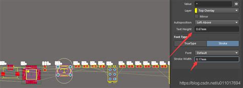
(16) Silkscreen layer
After the design of the unit board is completed, the unit board information should be marked on the TOP layer of the unit board, including the board number, basic parameters of the unit board, and completion date.
The unit board should have obvious cascade direction marks at prominent positions at the cascade entrance and cascade exit; there should be obvious marks at the 1-pin position of the cascade pin header and other pin headers; there should be easy-to-observe +- marks next to the positive and negative pins of the power socket, and there should be obvious indications of the soldering direction; for empty pads designed for jumpers, obvious network name labels should be placed; for unit boards with separate lamp boards and driver boards, there should be obvious plug-in direction indications on both the lamp board and the driver board, or asymmetric treatment should be made during design.
For components with positive and negative poles, the direction of the positive and negative poles should be reflected on the layout. Such as diodes, voltage regulators, electrolytic capacitors, power sockets, etc., and the direction of placement cannot be covered after welding;
For virtual pixel unit boards, in addition to the welding direction of the LED, there must be obvious R/G/B signs. For unit boards with surface-mounted LED lights that cannot be silk-screened on the bottom layer, the arrangement of the LED lights must be detailed in the production instructions.
In order not to affect welding, the characters on the silk-screen layer cannot overlap with the pads.
After the drawing is completed, place the name of the IC under the IC; for 62706 or 595, place the color control mark next to the IC;
After the PCB design is completed, place optical positioning points on the diagonal of the PCB.
(17) Inspection
After the design is completed, DRC inspection must be performed. When converting to PROTEL2.8 after drawing with PROTEL99 and POWERPCB.
When importing into Protel2.8 format after drawing with PowerPCB software, it should be noted that sometimes the vias on the board will change size. After drawing with Protel99 software, when importing into Protel2.8 format, the vertically placed FILL may be changed to horizontal placement. These are things to pay attention to when drawing.
When drawing PCB, for components with positive and negative poles, the direction of the positive and negative poles must be reflected on the layout. Such as diodes, voltage regulators, electrolytic capacitors, power sockets, etc.
For two-pin components, you must not use the library of ordinary two-pin components of SIP2 or IDC2, and you must use a dedicated component library.
For power sockets or power pads, the network name (or positive and negative pole signs) must be marked on the silk screen layer.
For single-row and double-row needles, there must be a clear mark at the position of one pin.
For other components, there must be a clear 1-pin mark or welding direction mark.
For unconventional usage, it must be explained in the production instructions.
For unit boards with virtual pixels, in addition to the soldering direction of the LED, there must also be obvious R/G/B markings. For surface-mounted unit boards that cannot have the bottom layer silk-screened, detailed instructions must be given in the production instructions.