Let you know about the immersion gold process in PCB
The advantage of the immersion gold process is that the color deposited on the surface of the printed circuit is very stable, the brightness is very good, the coating is very flat, and the solderability is very good.
The thickness of the gold in the immersion gold is generally 1-3 Uinch, so the thickness of the gold made by the immersion gold surface treatment method is generally thicker, so the immersion gold surface treatment method is widely used in keypads, gold finger boards and other circuit boards, because gold has strong conductivity, good oxidation resistance and long service life.
PCB board immersion gold process flow:
I. Process introduction:
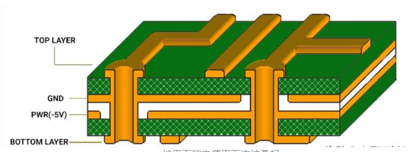
The purpose of the immersion gold process is to deposit a nickel-gold coating with stable color, good brightness, flat coating and good solderability on the surface of the printed circuit. It can be basically divided into four stages: pre-treatment (degreasing, micro-etching, activation, post-immersion), nickel immersion, immersion gold, post-treatment (waste gold water washing, DI water washing, drying).
2.Pretreatment:
The pretreatment of immersion gold generally has the following steps: degreasing (30% AD-482), microetching (60g/InaPS, 2% H2SO4), activation (10% Act-354-2), and post-immersion (1% H2S04). To remove the copper surface oxide, and precipitate palladium on the copper surface to serve as the activation center for immersion nickel. If any of these links is not handled properly, it will affect the subsequent immersion of nickel and immersion gold, and lead to batch scrapping. During the production process, various potions must be analyzed and replenished regularly and controlled within the required range. For example, the more important ones are: the microetching rate should be controlled at “25U-40U”, and a new tank must be opened when the copper content of the activation potion is greater than 800PPM. The cleaning and maintenance of the potion tank also has a greater impact on the quality of the PCB. The degreasing tank, microetching tank, and post-immersion tank should be replaced weekly, and each washing tank should also be cleaned weekly.
3.Nickel deposition:
and stabilizer. Since chemical nickel has strict requirements on the range of potion ingredients, it must be analyzed and tested twice per shift during the production process, and Ni? reducing agent should be added according to the bare copper area of the production board or experience.
When adding materials, the principle of small amounts and multiple dispersed additions should be followed to prevent local plating solution from reacting violently, causing the plating solution to age faster.
The pH value and plating solution temperature have a greater impact on nickel thickness. The nickel potion temperature is controlled at 85℃-90℃. When the pH is 5.3-5.7 and the nickel cylinder is not in production, the nickel cylinder temperature should be lowered to about 70℃ to slow down the aging of the plating solution.
Chemical nickel plating solution is sensitive to impurities, and many chemical components are harmful to chemical nickel, which can be divided into the following categories: Inhibitors: including Pb.Sn..Hg.Ti.Bi (heavy metals with low melting points).
4.Immersion gold:
The immersion gold process is a kind of immersion gold process.
The main components of the immersion gold tank are Au (1.5-3.5g/l) and the binder is (Ec0.06-0.16mol/L). It can replace the pure gold plating on the nickel-phosphorus alloy layer, making the coating smooth and finely crystallized. The pH value of the plating solution is generally between 4-5, and the temperature is controlled at 85-90 degrees Celsius.
5.Post-processing:
Post-processing is also an important link. For printed circuit boards, it generally includes: waste gold washing, DI washing, drying and other steps. If conditions permit, the immersion gold board can be further washed and dried with a horizontal board washer. The horizontal board washer can be set up in the order of chemical washing (10% sulfuric acid, 30g/L hydrogen peroxide), high-pressure DI washing (30-50PSI), DI washing, drying, and drying to completely remove the chemical and water stains in the holes and on the surface of the printed circuit board, and obtain a uniformly plated, bright immersion gold board.
Characteristics of PCB Immersion Gold Process
There is a very common process in the surface treatment of circuit boards, that is, the Immersion Gold process. The Immersion Gold process has very obvious characteristics, so let’s first analyze the characteristics of the surface treatment of Immersion Gold from the definition and practice of Immersion Gold.
- Definition of Immersion Gold. Simply put, Immersion Gold is a method of chemical deposition to produce a layer of metal plating on the surface of the circuit board through a chemical oxidation-reduction reaction.
- Characteristics of Immersion Gold Process. The copper on the circuit board is mainly red copper. The copper solder joints are easily oxidized in the air, which will cause poor conductivity, that is, poor tinning or poor contact, which reduces the performance of the circuit board. Then, the copper solder joints need to be surface treated. Immersion Gold is to plate gold on it. Gold can effectively block copper metal and air to prevent oxidation. Therefore, Immersion Gold is a treatment method for surface oxidation prevention. It is a layer of gold on the surface of copper through chemical reaction, also called chemical gold.
- Advantages of Immersion Gold Surface Treatment. The advantage of the Immersion Gold process is that the color of the surface deposit is very stable when the circuit is printed, the brightness is very good, the coating is very flat, and the solderability is very good. The thickness of gold in immersion gold is generally 1-3 Uinch, so the gold thickness made by immersion gold surface treatment is generally thicker, so immersion gold surface treatment is widely used in keypads, gold finger boards and other circuit boards, because gold has strong conductivity, good oxidation resistance and long service life.
- Characteristics of immersion gold board:
1) The immersion gold board has bright colors, good color and good appearance.
2) The crystal structure formed by immersion gold is easier to weld than other surface treatments, and can have better performance and ensure quality.
3) Because the immersion gold board only has nickel gold on the pad, it will not affect the signal, because the signal transmission in the skin effect is in the copper layer.
4) The metal properties of gold are relatively stable, the crystal structure is denser, and it is not easy to oxidize.
5) Because the immersion gold board only has nickel gold on the pad, the combination of the solder mask and the copper layer on the circuit is more solid, and it is not easy to cause micro short circuit.
6) The engineering will not affect the spacing when making compensation.
7) The stress of the immersion gold board is easier to control.

5.The relationship between immersion gold and gold fingers
What is a gold finger (connecting finger)?
To put it bluntly, it is a brass contact, or a conductor. In detail, because gold has strong anti-oxidation and strong conductivity, the parts connected to the memory slot on the memory stick are plated with gold, and all signals are transmitted through the gold finger. Because the gold finger is composed of many yellow conductive contacts, its surface is plated with gold and the conductive contacts are arranged like fingers, hence the name.
In layman’s terms, the gold finger is the connecting part between the memory stick and the memory slot, and all signals are transmitted through the gold finger.
The gold finger is composed of many golden conductive contacts. The gold finger is actually a layer of gold coated on the copper clad board through a special process.
Therefore, the simple distinction is that immersion gold is a surface treatment process for the circuit board, and the gold finger is a component on the circuit board that has signal connection and conduction. In the actual market, the gold finger may not be actually gold on the surface.
Because of the high price of gold, most memory is now replaced by tin plating. Since the 1990s, tin materials have become popular. At present, the “gold fingers” of motherboards, memory and graphics cards are almost all made of tin materials. Only the contact points of accessories of some high-performance servers/workstations will continue to use gold plating, which is naturally expensive.
What kind of PCB board needs immersion gold and gold fingers
First of all, let’s introduce what is immersion gold? The copper on the circuit board is mainly red copper. The copper solder joints are easily oxidized in the air, which will cause poor conductivity, that is, poor tinning or poor contact, which reduces the performance of the circuit board. Then, the copper solder joints need to be surface treated. Immersion gold is to plate gold on it. Gold can effectively block copper metal and air to prevent oxidation. Therefore, immersion gold is a treatment method for surface oxidation prevention. It is a layer of gold on the surface of copper through chemical reaction, also called gold.
So what is a gold finger?
Let’s say it more bluntly, it is a brass contact, or a conductor. Specifically, it is the part on the memory stick that is connected to the memory slot. All signals are transmitted through gold fingers. It is composed of many yellow conductive contacts. Its surface is gold-plated and the conductive contacts are arranged like fingers, hence the name.
The advantage of the immersion gold process is that the color of the deposit on the surface is very stable when printing circuits, the brightness is very good, the coating is very flat, and the solderability is very good.
Generally, the thickness of immersion gold is 1-3 Uinch, which can be basically completed in four stages: pre-treatment (degreasing, micro-etching, activation, post-immersion), nickel immersion, immersion gold, and post-treatment (waste gold washing, DI washing, drying).
However, compared with other tin-spraying processes, the immersion gold process is more expensive in terms of production costs.
If the thickness of gold exceeds the conventional process of the plate-making factory, the cost will be even more expensive. Of course, if you have higher requirements for the solderability and electrical properties of the board, it is another matter. For example: if your circuit board has gold fingers that need to be immersing gold, or if the line width/pad spacing of the board is insufficient, then it is best to use the process of immersion gold + gold-plated fingers. In this way, the circuit board welding is very good, the circuit board performance is also very stable, the pad will not fall off, the contact will not be bad, there will be no short circuit and other phenomena, and it is also very shockproof and drop-proof. Of course, we will not drop the board.
Another situation is that the circuit board has gold fingers, but the board surface other than the gold fingers can choose the tin spraying process according to the situation, that is, the tin spraying + gold-plated finger process. When the line width of the circuit board and the pad spacing are sufficient and the welding requirements are not high, it can effectively reduce the production cost without affecting the use of the board. However, if the line width of the board and the pad spacing are insufficient, then the use of the tin spraying process in this case will increase the production difficulty greatly, and there will be more short circuits such as tin bridging, and the gold fingers will often be inserted and stripped, resulting in poor contact.
Therefore, we can choose the board making process that suits us according to the actual situation of our own circuit board, which controls the cost and does not affect the use of the board.