Low-Power System Design Using FPGAs
The combination of low-power components and low-power design techniques is more valuable now than ever before. As components integrate more functions and become smaller, the demand for low power continues to grow. When using programmable logic devices for low-power applications, it is important to limit the low power consumption of the design. This article will discuss various methods to reduce dynamic and static power consumption and provide some examples of how to minimize power consumption.
The three main sources of power consumption are startup, standby, and dynamic power.
The current associated with the device when it is powered on is the startup current; standby power, also known as static power, is the power consumption of the device when the power is on but there is no switching activity on the I/O; and dynamic power is the power consumption of the device when it is operating normally.
The startup current varies from device to device.
For example, SRAM-based FPGAs have high startup currents because these devices are not configured when they are first powered on and need to download data from external memory chips to configure their programmable resources, such as routing connections and lookup tables. In contrast, anti-fuse FPGAs do not require power-on configuration and therefore do not have high startup currents.
Like startup current, standby power consumption depends primarily on the electronic characteristics of the device.
Because the number of SRAM cells in the SRAM FPGA interconnect is quite large, they consume hundreds of milliamps of current even in standby. Antifuse FPGAs have metal-to-metal interconnects that do not require additional transistors to maintain the interconnects, and therefore do not generate additional power. However, for both types of FPGAs, leakage current will increase as the process geometry shrinks, which exacerbates the power consumption problem.
Another challenge is dynamic power consumption, which can be several times greater than standby power consumption.
Dynamic power consumption is proportional to the frequency of charging and discharging parasitic capacitances of FPGA internal cells (such as registers and combinational logic), so it is usually optimized for the design.
The following are some common techniques for reducing power consumption in FPGA design:
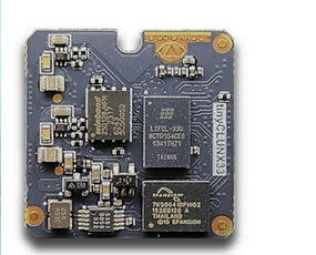
Low-power system design techniques using FQGA
- State machine encoding. A large number of logic resources are defined by the type of finite state machine implemented. One-hlt state machine encoding creates a state machine with one flip-flop for each state. Compared with Gray and binary state machines, less use of one-hot state machines can obtain more power-efficient designs. Some synthesizer software can automatically encode state machines, but the most efficient approach is to define state values directly in the HDL code.
- Guard assignments. The key to guarding assignments is to prevent input signals from propagating down to other logic blocks if the final output does not need to be updated. Guarding input signals ensures that output values are changed only when appropriate, minimizing unnecessary output switching.
Adding latches to the inputs of large combinatorial logic (such as wide bus multiplexers) can inhibit invalid switching activity because the inputs are latched only when the outputs need to be updated. Similarly, control registers can be used to turn low-level modules (such as state machines in submodules) on or off. Keeping large buses and submodules in a constant state helps reduce the number of unrelated output switches.
- Combinatorial loops. Designers may occasionally create combinatorial loops in FPGA designs without noticing. These loops are formed when a group of related combinatorial logic keeps oscillating under certain conditions. Oscillators consume a lot of current in FPGAs. Therefore, it is best to evaluate the oscillator or ensure that any feedback logic is gated by a register before re-evaluating.
- Gated clocks. The system can slow down or stop the clocks of modules that are not used temporarily. At any given time, power can be saved by clocking. Gated clocks can significantly save power because the number of active clock buffers is reduced, the number of flip-flops toggled will be reduced, and the outputs of those flip-flops will be less likely to invert. Gated clocks require careful planning and partitioning of the algorithm, but the power savings are considerable.

Power saving methods for system-level applications:
- System clock speed. The system clock frequency has a significant impact on the overall power consumption of the board because the clock signal has the most switching activity and the largest capacitive loading. However, clock speed is directly related to bandwidth performance. To achieve an optimal balance between power consumption and throughput, designers can provide slower clocks to components that do not require fast clocks, fast clocks to components that are critical to bandwidth, or use a built-in phase-locked loop to generate a fast clock for specific modules that require high-speed performance.
- Component enablement. Sometimes, outputs are assigned even if their behavior is not necessary for the current function. To reduce the excess power consumption of unused I/O, a system controller can be mapped to the FPGA to shut down temporarily unused devices. When a device is not relevant to the current operation, the system controller can remove its use signal; or, if the device will not be accessed for a long time, it can be put into sleep mode. Implementing such a system controller in a low-power FPGA can reduce the total switching activity of the system and intelligently keep some temporarily unused devices in sleep mode. Component enable is similar to assignment protection, except that component enable is implemented at the system level and it controls the components on the board rather than the modules in the FPGA.
- Intelligent coprocessor. Generally speaking, LCD screens and microprocessors occupy most of the power budget in the design,
Therefore, power consumption is often saved by reducing the brightness of the LCD screen or partially turning off the screen. Similarly, keeping the microprocessor in sleep mode can also extend battery life.
Unfortunately, microprocessors usually need to handle interrupt service routines for multiple devices, which makes it difficult for the microprocessor to be in sleep mode. Given this, offloading tasks such as peripheral oscillation and interrupt control to a low-power FPGA can greatly reduce power consumption. A low-power interrupt controller or data coprocessor implemented in the FPGA can handle some interrupt activities by itself, so it can avoid waking up the microprocessor for low-priority activities.
For systems that strictly require low power consumption, using appropriate low-power programmable logic devices and power-saving design techniques can help minimize system power consumption.