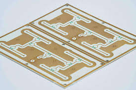
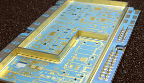
ltcc ceramic pcb
Advantages Of LTCC Ceramic PCB In High-Frequency Applications
Low-Temperature Co-fired Ceramic (LTCC) technology has emerged as a pivotal innovation in the realm of high-frequency applications, offering a multitude of advantages that make it an ideal choice for modern electronic devices. As the demand for high-performance, miniaturized, and reliable electronic components continues to grow, LTCC ceramic PCBs have become increasingly significant due to their unique properties and capabilities.
One of the primary advantages of LTCC ceramic PCBs is their excellent thermal stability.
Unlike traditional organic substrates, LTCC materials can withstand high temperatures without degrading, making them particularly suitable for high-frequency applications where heat generation is a concern. This thermal resilience ensures that the electronic components maintain their performance and reliability over extended periods, even under challenging conditions. Furthermore, the inherent thermal conductivity of ceramic materials facilitates efficient heat dissipation, which is crucial for maintaining the integrity and functionality of high-frequency circuits.
In addition to thermal stability, LTCC ceramic PCBs offer superior electrical properties that are essential for high-frequency applications.
The low dielectric constant and low loss tangent of LTCC materials contribute to minimal signal loss and distortion, which are critical factors in maintaining signal integrity at high frequencies. This characteristic is particularly beneficial in applications such as RF and microwave circuits, where precise signal transmission is paramount. Moreover, the ability to integrate passive components such as resistors, capacitors, and inductors directly into the LTCC substrate further enhances the performance and compactness of the circuit, reducing the need for additional discrete components and interconnections.
Another significant advantage of LTCC ceramic PCBs is their mechanical robustness.
The ceramic substrate provides a sturdy foundation that is resistant to mechanical stress and environmental factors such as moisture and chemical exposure. This durability ensures that the PCBs can withstand harsh operating environments, making them suitable for use in aerospace, automotive, and industrial applications where reliability is non-negotiable. Additionally, the co-firing process used in LTCC manufacturing allows for the creation of multilayer structures, enabling complex circuit designs with multiple layers of interconnections. This capability not only enhances the functionality of the PCB but also contributes to the miniaturization of electronic devices, a key requirement in today’s technology-driven world.
Furthermore, LTCC technology offers significant design flexibility, allowing engineers to tailor the PCB to specific application requirements.
The ability to customize the dielectric properties, layer thickness, and conductor materials provides a high degree of control over the electrical and mechanical characteristics of the final product. This adaptability is particularly advantageous in high-frequency applications where precise tuning of the circuit parameters is necessary to achieve optimal performance.
In conclusion, the advantages of LTCC ceramic PCBs in high-frequency applications are manifold, encompassing thermal stability, superior electrical properties, mechanical robustness, and design flexibility. These attributes make LTCC technology an indispensable tool in the development of advanced electronic systems that demand high performance and reliability. As the landscape of electronic applications continues to evolve, the role of LTCC ceramic PCBs is poised to expand, driving innovation and enabling the next generation of high-frequency devices.

Manufacturing Process Of LTCC Ceramic PCB: A Step-By-Step Guide
The manufacturing process of Low-Temperature Co-fired Ceramic (LTCC) Printed Circuit Boards (PCBs) is a sophisticated procedure that involves several meticulous steps, each contributing to the creation of a highly reliable and efficient electronic substrate. LTCC technology is renowned for its ability to integrate passive components directly into the ceramic substrate, offering significant advantages in terms of miniaturization, performance, and thermal management. Understanding the step-by-step process of manufacturing LTCC ceramic PCBs is essential for appreciating the complexity and precision involved in their production.
Initially, the process begins with the preparation of ceramic tapes, which serve as the foundational material for LTCC PCBs.
These tapes are composed of ceramic powders mixed with organic binders and solvents, forming a pliable sheet. The selection of ceramic materials is crucial, as it determines the electrical and thermal properties of the final product. Once the ceramic tapes are prepared, they undergo a drying process to remove excess solvents, ensuring the tapes are ready for subsequent processing.
Following the preparation of ceramic tapes, the next step involves the creation of circuit patterns through a process known as screen printing.
This technique employs a stencil or screen to apply conductive pastes onto the ceramic tapes, forming the desired circuit layout. The conductive pastes typically consist of metal particles suspended in a binder, which, upon firing, will form the conductive traces and pads necessary for electrical connectivity. Screen printing is a critical step, as it defines the electrical pathways and interconnections within the LTCC PCB.
Subsequently, the printed ceramic tapes are stacked and laminated to form a multi-layer structure.
This step is essential for achieving the desired circuit complexity and functionality. The alignment of each layer is meticulously controlled to ensure precise registration of the circuit patterns. Once aligned, the layers are pressed together under heat and pressure, causing the organic binders to soften and bond the layers into a cohesive unit. This lamination process is pivotal in creating a robust and reliable multi-layer LTCC substrate.
After lamination, the stacked and bonded ceramic tapes undergo a firing process in a controlled atmosphere.
This step, known as co-firing, involves heating the laminated structure to a temperature typically below 1000°C. During co-firing, the organic binders are burned off, and the ceramic particles sinter together, forming a dense and solid ceramic substrate. The co-firing process is critical, as it determines the mechanical strength and electrical properties of the LTCC PCB.
Once the co-firing is complete, the LTCC substrate is ready for post-processing steps, which may include the addition of surface finishes, vias, and other necessary features.
Vias are created to establish electrical connections between different layers of the substrate, and they are typically filled with conductive materials to ensure reliable inter-layer connectivity. Surface finishes, such as gold or silver plating, may be applied to enhance solderability and protect the conductive traces from oxidation.
In conclusion, the manufacturing process of LTCC ceramic PCBs is a complex and precise procedure that involves multiple steps, each contributing to the creation of a high-performance electronic substrate. From the preparation of ceramic tapes to the final post-processing steps, each stage requires careful attention to detail and adherence to stringent quality standards. The result is a versatile and reliable LTCC PCB that meets the demanding requirements of modern electronic applications.
Comparing LTCC Ceramic PCB With Other Substrate Technologies
Low Temperature Co-fired Ceramic (LTCC) technology has emerged as a significant player in the realm of printed circuit boards (PCBs), offering distinct advantages over other substrate technologies. To understand the unique position of LTCC ceramic PCBs, it is essential to compare them with other prevalent substrate technologies such as FR-4, HTCC (High Temperature Co-fired Ceramic), and alumina substrates. Each of these technologies has its own set of characteristics, making them suitable for specific applications, yet LTCC stands out due to its unique properties.
Firstly, when comparing LTCC with the widely used FR-4 substrate, the differences in thermal and electrical performance become apparent.
FR-4, a composite material made of woven fiberglass cloth with an epoxy resin binder, is known for its cost-effectiveness and versatility. However, it falls short in high-frequency applications due to its relatively high dielectric loss. In contrast, LTCC ceramic PCBs offer superior dielectric properties, making them ideal for high-frequency and microwave applications. Additionally, LTCC can withstand higher temperatures, which enhances its reliability in harsh environments where FR-4 might degrade.
Transitioning to a comparison with HTCC, both LTCC and HTCC are ceramic-based technologies, yet they differ significantly in their processing temperatures and material compositions.
HTCC involves higher sintering temperatures, which can limit the choice of materials and increase production costs. LTCC, on the other hand, is processed at lower temperatures, allowing for the integration of a wider range of materials, including low-resistance conductors like silver and gold. This flexibility in material selection not only reduces costs but also enhances the performance of the final product. Moreover, LTCC’s ability to integrate passive components such as resistors, capacitors, and inductors directly into the substrate offers a level of miniaturization and functionality that HTCC cannot easily achieve.
Furthermore, when considering alumina substrates, which are often used in applications requiring excellent thermal conductivity, LTCC provides a competitive alternative.
While alumina offers high thermal conductivity, it lacks the ability to integrate multiple layers and components as efficiently as LTCC. The multi-layer capability of LTCC allows for more complex circuit designs and greater functionality within a smaller footprint. This is particularly advantageous in modern electronic devices where space is at a premium.
In addition to these comparisons, it is important to highlight the environmental and economic aspects of LTCC technology.
The lower processing temperatures of LTCC not only reduce energy consumption but also minimize the environmental impact associated with manufacturing. Economically, while the initial cost of LTCC may be higher than that of traditional substrates like FR-4, the long-term benefits in terms of performance, reliability, and integration capabilities often justify the investment.
In conclusion, LTCC ceramic PCBs offer a compelling combination of high-frequency performance, material flexibility, and integration capabilities that make them a superior choice in many applications compared to other substrate technologies. While each substrate technology has its own strengths and ideal use cases, LTCC’s unique properties position it as a versatile and efficient solution for modern electronic demands. As technology continues to advance, the role of LTCC in the development of innovative electronic systems is likely to expand, further solidifying its place in the industry.
Innovations In LTCC Ceramic PCB For Miniaturized Electronic Devices
Low Temperature Co-fired Ceramic (LTCC) technology has emerged as a pivotal innovation in the realm of miniaturized electronic devices, offering a host of advantages that cater to the ever-evolving demands of modern electronics. As the quest for smaller, more efficient, and highly reliable electronic components intensifies, LTCC ceramic PCBs have become a cornerstone in achieving these objectives. This technology, characterized by its ability to integrate multiple passive components into a single substrate, is revolutionizing the design and functionality of compact electronic devices.
One of the primary benefits of LTCC ceramic PCBs is their exceptional thermal stability.
Unlike traditional PCBs, which may suffer from performance degradation at high temperatures, LTCC substrates maintain their integrity and functionality across a wide temperature range. This makes them particularly suitable for applications in harsh environments, such as automotive and aerospace industries, where temperature fluctuations are a common challenge. Furthermore, the inherent thermal conductivity of ceramic materials ensures efficient heat dissipation, thereby enhancing the reliability and longevity of electronic components.
In addition to thermal advantages, LTCC technology offers superior electrical performance.
The low dielectric constant and loss tangent of ceramic materials contribute to reduced signal loss and improved high-frequency performance. This is particularly beneficial in the development of RF and microwave circuits, where signal integrity is paramount. The ability to integrate passive components such as resistors, capacitors, and inductors directly into the LTCC substrate further enhances the electrical performance by minimizing parasitic effects and reducing the overall footprint of the circuit.
Moreover, the miniaturization potential of LTCC ceramic PCBs is a significant driving force behind their adoption in modern electronic devices.
As consumer electronics continue to shrink in size while increasing in functionality, the demand for compact and efficient circuit solutions has never been greater. LTCC technology allows for the creation of multi-layered circuits with high component density, enabling the development of smaller, lighter, and more portable devices without compromising on performance. This is particularly advantageous in the design of wearable technology, medical implants, and other applications where space is at a premium.
The versatility of LTCC ceramic PCBs also extends to their mechanical properties.
The robust nature of ceramic materials provides excellent resistance to mechanical stress, vibration, and chemical exposure, making them ideal for use in demanding environments. This durability ensures that devices can withstand the rigors of daily use and maintain their performance over time, a critical factor in the reliability of electronic products.
Furthermore, the environmental benefits of LTCC technology cannot be overlooked.
The manufacturing process of LTCC ceramic PCBs is relatively eco-friendly, as it involves fewer hazardous materials compared to traditional PCB production. This aligns with the growing emphasis on sustainable practices within the electronics industry, as manufacturers seek to reduce their environmental footprint while meeting consumer expectations for greener products.
In conclusion, the innovations in LTCC ceramic PCB technology are playing a crucial role in the advancement of miniaturized electronic devices. By offering unparalleled thermal stability, electrical performance, miniaturization potential, mechanical robustness, and environmental benefits, LTCC technology is setting new standards in the design and functionality of modern electronics. As the demand for smaller, more efficient devices continues to grow, LTCC ceramic PCBs are poised to remain at the forefront of this technological evolution, driving further advancements and opening new possibilities in the world of electronics.


