Manufacturers of hdi pcb
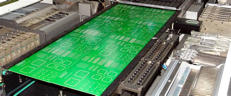
Innovations In HDI PCB Manufacturing Techniques
High-Density Interconnect (HDI) printed circuit boards (PCBs) have become a cornerstone in the advancement of modern electronics, driven by the demand for more compact, efficient, and powerful devices. As the electronics industry continues to evolve, manufacturers of HDI PCBs are at the forefront of innovation, employing cutting-edge techniques to meet the ever-increasing requirements of various sectors, including telecommunications, consumer electronics, and automotive industries. These innovations are not only enhancing the performance and reliability of electronic devices but also pushing the boundaries of what is technologically possible.
One of the most significant advancements in HDI PCB manufacturing is the development of laser drilling technology.
This technique allows for the creation of microvias, which are essential for the high-density interconnects that characterize HDI PCBs. Laser drilling offers precision and accuracy that traditional mechanical drilling cannot achieve, enabling the production of smaller and more densely packed vias. This advancement is crucial for manufacturers aiming to reduce the size of PCBs while increasing their functionality. Moreover, laser drilling contributes to improved signal integrity and reduced electrical losses, which are critical factors in the performance of high-speed electronic devices.
In addition to laser drilling, the use of advanced materials has also played a pivotal role in the evolution of HDI PCB manufacturing.
Manufacturers are increasingly turning to materials such as liquid crystal polymer (LCP) and polytetrafluoroethylene (PTFE) to enhance the thermal and electrical properties of PCBs. These materials offer superior dielectric properties and thermal stability, which are essential for the reliable operation of high-frequency and high-power applications. By incorporating these advanced materials, manufacturers can produce HDI PCBs that not only meet but exceed the stringent performance requirements of modern electronic devices.
Furthermore, the adoption of additive manufacturing techniques, such as 3D printing, is revolutionizing the way HDI PCBs are designed and produced.
This innovative approach allows for greater design flexibility and customization, enabling manufacturers to create complex geometries and structures that were previously unattainable with traditional subtractive methods. Additive manufacturing also reduces material waste and production time, leading to more sustainable and cost-effective manufacturing processes. As a result, manufacturers can respond more swiftly to market demands and deliver high-quality products with shorter lead times.
Another noteworthy innovation in HDI PCB manufacturing is the implementation of advanced inspection and testing technologies.
Automated optical inspection (AOI) and X-ray inspection systems are now integral to the quality assurance process, ensuring that each PCB meets the highest standards of precision and reliability. These technologies allow manufacturers to detect and rectify defects at an early stage, minimizing the risk of failures in the final product. Consequently, the integration of these inspection systems enhances the overall quality and dependability of HDI PCBs, which is paramount in applications where failure is not an option.
In conclusion, the landscape of HDI PCB manufacturing is continually being reshaped by a series of technological innovations.
From laser drilling and advanced materials to additive manufacturing and sophisticated inspection systems, these advancements are enabling manufacturers to produce PCBs that are smaller, more efficient, and more reliable than ever before. As the demand for high-performance electronic devices continues to grow, manufacturers of HDI PCBs will undoubtedly remain at the cutting edge of technology, driving further innovations that will shape the future of the electronics industry.
Leading HDI PCB Manufacturers: A Global Overview
High-Density Interconnect (HDI) printed circuit boards (PCBs) have become a cornerstone in the electronics industry, driving advancements in technology by enabling more compact and efficient designs. As the demand for smaller, faster, and more powerful electronic devices continues to grow, the role of HDI PCB manufacturers becomes increasingly critical. This article provides a global overview of leading HDI PCB manufacturers, highlighting their contributions to the industry and the innovations they bring to the table.
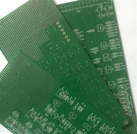
To begin with, it is essential to understand what sets HDI PCBs apart from traditional PCBs.
HDI PCBs are characterized by their higher wiring density per unit area, which is achieved through the use of finer lines and spaces, smaller vias, and capture pads. This allows for more components to be placed on both sides of the board, significantly enhancing the performance and functionality of electronic devices. Consequently, manufacturers specializing in HDI PCBs are at the forefront of technological innovation, catering to industries such as telecommunications, consumer electronics, automotive, and healthcare.
One of the leading names in the HDI PCB manufacturing sector is TTM Technologies, a global leader known for its extensive capabilities in producing advanced PCBs.
With a strong presence in North America, Asia, and Europe, TTM Technologies offers a wide range of HDI solutions that cater to various market needs. Their commitment to research and development ensures that they remain at the cutting edge of technology, providing customers with high-quality products that meet the ever-evolving demands of the electronics industry.
Similarly, Unimicron Technology Corporation, based in Taiwan, is another prominent player in the HDI PCB market.
As one of the largest PCB manufacturers in the world, Unimicron has made significant investments in state-of-the-art facilities and advanced manufacturing processes. This enables them to produce HDI PCBs with exceptional precision and reliability, making them a preferred choice for many leading electronics companies. Their focus on sustainability and environmental responsibility further enhances their reputation as a forward-thinking manufacturer.
In addition to these giants, AT&S, an Austrian company, has carved out a niche for itself in the HDI PCB landscape.
Known for their high-quality products and innovative solutions, AT&S has established itself as a trusted partner for industries requiring advanced PCB technologies. Their expertise in miniaturization and high-frequency applications makes them a valuable asset in the development of next-generation electronic devices.
Moreover, the Asian market is home to several other key players, such as Zhen Ding Technology Holding Limited and Compeq Manufacturing Co., Ltd. These companies have leveraged their strategic locations and access to cutting-edge technology to become leaders in the HDI PCB industry. Their ability to deliver cost-effective solutions without compromising on quality has made them indispensable partners for global electronics manufacturers.
As we look to the future, the role of HDI PCB manufacturers will only become more significant.
The ongoing trends of miniaturization, increased functionality, and the Internet of Things (IoT) will continue to drive demand for advanced PCBs. Manufacturers that can adapt to these changes and invest in innovative technologies will be well-positioned to lead the industry. In conclusion, the global landscape of HDI PCB manufacturers is marked by a blend of established leaders and emerging innovators, all contributing to the rapid evolution of electronic technology. Their collective efforts ensure that the world remains connected, efficient, and ever-progressing.
Challenges Faced By HDI PCB Manufacturers And Solutions
High-Density Interconnect (HDI) printed circuit boards (PCBs) have become a cornerstone in the advancement of modern electronics, offering enhanced performance and miniaturization capabilities. However, the manufacturing of HDI PCBs presents a unique set of challenges that manufacturers must navigate to meet the increasing demands of the industry. Understanding these challenges and exploring potential solutions is crucial for manufacturers striving to maintain competitiveness and innovation in this rapidly evolving field.
One of the primary challenges faced by HDI PCB manufacturers is the complexity of the design and fabrication processes.
HDI PCBs are characterized by their high wiring density, which requires precise and intricate design layouts. This complexity often leads to increased design time and higher costs, as manufacturers must invest in advanced design software and skilled personnel to ensure accuracy. To address this, manufacturers are increasingly adopting automated design tools that leverage artificial intelligence and machine learning to optimize design processes, thereby reducing time and cost while maintaining high precision.
In addition to design complexities, the miniaturization of components poses significant manufacturing challenges. As electronic devices become smaller, the demand for compact and efficient PCBs grows. This necessitates the use of microvias, fine lines, and spaces, which require advanced manufacturing techniques and equipment. The implementation of laser drilling technology has emerged as a solution, enabling the creation of microvias with high precision and reliability. Furthermore, manufacturers are investing in state-of-the-art equipment that supports finer line widths and tighter tolerances, ensuring that the miniaturization requirements are met without compromising quality.
Material selection is another critical challenge in HDI PCB manufacturing.
The materials used must possess excellent thermal and electrical properties to support the high-density interconnections. However, finding materials that meet these criteria while remaining cost-effective can be difficult. Manufacturers are exploring innovative materials such as advanced laminates and substrates that offer superior performance characteristics. Additionally, collaboration with material suppliers to develop customized solutions tailored to specific application needs is becoming increasingly common, allowing manufacturers to achieve the desired balance between performance and cost.
Quality control and testing present further challenges in the production of HDI PCBs.
The intricate nature of these boards makes it difficult to detect defects and ensure reliability. Traditional testing methods may not be sufficient to identify issues in such complex designs. To overcome this, manufacturers are adopting advanced inspection technologies, such as automated optical inspection (AOI) and X-ray inspection, which provide comprehensive analysis and detection capabilities. These technologies enable manufacturers to identify defects early in the production process, reducing waste and improving overall product quality.
Finally, the rapid pace of technological advancements in the electronics industry necessitates continuous innovation and adaptation by HDI PCB manufacturers.
Staying abreast of emerging trends and technologies is essential to remain competitive. Manufacturers are increasingly investing in research and development to explore new manufacturing techniques and materials that can enhance the performance and capabilities of HDI PCBs. Additionally, fostering partnerships with research institutions and industry consortia can provide valuable insights and collaborative opportunities, driving innovation and ensuring that manufacturers remain at the forefront of the industry.
In conclusion, while the challenges faced by HDI PCB manufacturers are significant, they are not insurmountable. Through the adoption of advanced technologies, strategic material selection, rigorous quality control, and a commitment to innovation, manufacturers can effectively address these challenges and continue to deliver high-performance solutions that meet the evolving needs of the electronics industry.
The Future Of HDI PCB Manufacturing: Trends And Predictions
The future of HDI (High-Density Interconnect) PCB manufacturing is poised for significant transformation, driven by technological advancements and evolving market demands. As the electronics industry continues to push the boundaries of innovation, HDI PCBs are becoming increasingly critical due to their ability to support complex circuitry in compact spaces. This trend is expected to accelerate, with several key factors shaping the future landscape of HDI PCB manufacturing.
To begin with, the demand for miniaturization in electronic devices is a primary driver of HDI PCB advancements.
As consumer electronics, such as smartphones, wearables, and IoT devices, become more sophisticated, the need for smaller, more efficient circuit boards intensifies. HDI PCBs, with their fine lines and microvias, offer the perfect solution by enabling higher component density and improved electrical performance. Consequently, manufacturers are investing in cutting-edge technologies to produce even more compact and efficient HDI PCBs, which will likely lead to further miniaturization of electronic devices.
Moreover, the rise of 5G technology is another significant factor influencing HDI PCB manufacturing.
The deployment of 5G networks requires electronic components that can handle higher frequencies and faster data transmission rates. HDI PCBs are well-suited for this purpose, as they provide the necessary signal integrity and thermal management capabilities. As 5G technology becomes more widespread, manufacturers are expected to focus on developing HDI PCBs that can meet the stringent requirements of 5G applications, thereby driving innovation in materials and design processes.
In addition to technological advancements, sustainability is becoming an increasingly important consideration in HDI PCB manufacturing.
As environmental concerns grow, manufacturers are under pressure to adopt eco-friendly practices and materials. This shift towards sustainability is likely to influence the choice of materials used in HDI PCBs, with a focus on reducing the environmental impact of production processes. For instance, the use of lead-free solder and halogen-free laminates is expected to become more prevalent, aligning with global environmental regulations and consumer expectations.
Furthermore, the integration of artificial intelligence (AI) and machine learning in the manufacturing process is set to revolutionize HDI PCB production.
These technologies can optimize design processes, improve quality control, and enhance production efficiency. By leveraging AI, manufacturers can predict potential defects, streamline production workflows, and reduce waste, ultimately leading to cost savings and improved product quality. As AI technology continues to evolve, its application in HDI PCB manufacturing is expected to expand, offering new opportunities for innovation and efficiency.
Lastly, the global supply chain dynamics are likely to impact the future of HDI PCB manufacturing.
The recent disruptions caused by the COVID-19 pandemic have highlighted the vulnerabilities in global supply chains, prompting manufacturers to reassess their strategies. As a result, there may be a shift towards localized production and diversification of supply sources to mitigate risks. This trend could lead to increased investment in domestic manufacturing capabilities and a focus on building resilient supply chains for HDI PCBs.
In conclusion, the future of HDI PCB manufacturing is set to be shaped by a combination of technological advancements, market demands, and sustainability considerations. As manufacturers adapt to these changes, they will need to embrace innovation and invest in new technologies to remain competitive. The ongoing evolution of HDI PCBs will undoubtedly play a crucial role in the advancement of electronic devices, paving the way for a more connected and efficient world.


