Mastering Board PCB Assembly: A Comprehensive Guide to Success
Key Takeaways
Understanding the intricacies of pcb assembly is crucial for anyone looking to excel in electronics. A solid foundation in the principles of PCB design is essential, as it lays the groundwork for creating effective and functional assemblies. Essential tools such as soldering irons, multimeters, and pcba components must be readily available to ensure smooth processes during assembly. A step-by-step approach to soldering techniques can significantly enhance the quality of your work. While challenges in pcb assembly, including misalignment and component placement errors, may arise, familiarizing oneself with common issues and their solutions can aid in overcoming them efficiently. Implementing robust quality control measures will allow you to maintain a flawless assembly process, which is vital for the success of any electronic project. As you advance into more complex designs, exploring advanced techniques will broaden your capabilities, enabling you to tackle innovative projects confidently. Lastly, keeping an eye on future trends in pcb assembly technology will help you stay ahead in this ever-evolving field, ensuring that your skills remain relevant and competitive.
Understanding PCB Design Principles
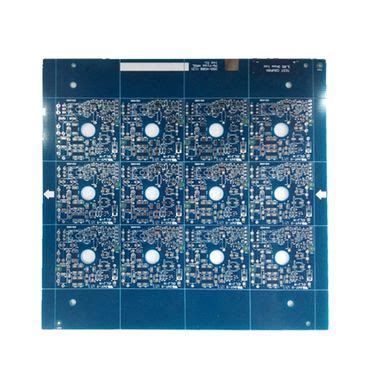
At the heart of successful pcb assembly lies the fundamental understanding of PCB design principles. This critical knowledge not only guides how a circuit board is created but also influences its functionality and reliability in electronic devices. A well-designed Printed Circuit Board (PCB) can significantly streamline the assembly process and reduce the chances of defects in the final product.
When designing a PCB, several key factors must be considered to optimize the pcba process:
| Design Factor | Description |
|---|---|
| Layer Count | Determines complexity and cost; consider whether single or multilayer boards are necessary. |
| Trace Width and Spacing | Essential for current carrying capacity; wider traces reduce resistance but also take more space. |
| Component Placement | Impacts signal integrity and ease of assembly; components should be placed logically for efficient soldering. |
| Ground Planes | Provide stable reference points in high-frequency designs, improving signal integrity. |
| Via Types and Placement | Vias must be strategically placed to minimize complexity while maintaining connectivity between layers. |
Incorporating these elements effectively contributes to a seamless transition from design to physical assembly, allowing for more effective soldering techniques and minimizing common issues that may arise during production.
“A well-structured design not only enhances performance but also simplifies the tasks for manufacturers during assembly.”
This quote emphasizes that understanding these design principles can make all the difference in achieving a smooth and successful assembly process. By mastering PCB design, both novice and experienced engineers can elevate their projects, leading to robust end products that meet consumer needs efficiently. Ultimately, adhering to strong design principles is invaluable as it lays the groundwork for all subsequent steps in the pcb assembly journey, ensuring that each board functions as intended in its final application.
Essential Tools and Materials for Board PCB Assembly
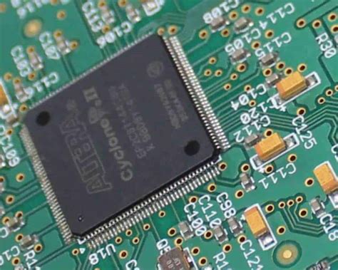
To successfully embark on the journey of pcb assembly, having the right tools and materials is paramount. The foundation of any pcba project starts with quality raw materials, including copper-clad laminates, which form the substrate for the PCB itself. You will also need a reliable soldering iron, ideally with adjustable temperature settings, to ensure optimal soldering without damaging sensitive components. Other essential tools include tweezers for placing small components, wire cutters for trimming leads, and a multimeter to verify electrical connectivity after assembly. For those interested in more advanced pcb assembly processes, investing in a reflow oven can enhance production efficiency and accuracy.
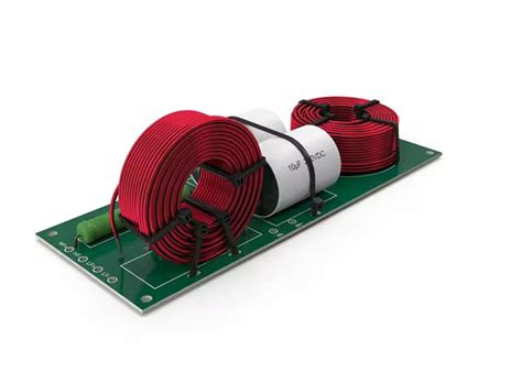
Moreover, the use of high-quality connectors, capacitors, resistors, and integrated circuits is crucial to ensuring that your final pcba meets performance expectations. It’s also wise to incorporate a well-organized workspace with proper lighting to facilitate precision during assembly. Having an adequate supply of solder wire and flux is essential as well, as they promote stronger connections between components. By assembling these tools and materials thoughtfully, you set yourself up for success in the meticulous world of pcb assembly. Remember that each project may require specific additional tools or components based on its complexity and purpose, so always plan according to your project’s unique needs.
Step-by-Step Guide to Soldering Techniques
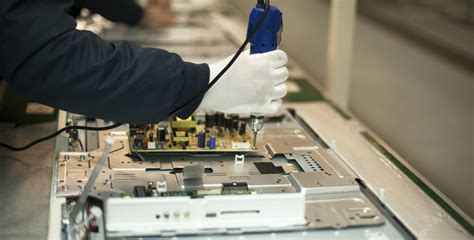
Soldering is a crucial skill in pcb assembly that requires precision and practice to master. To begin, ensure you have the right tools, such as a quality soldering iron, solder wire, and a reliable soldering mat. Start with your pcba components laid out according to your design specifications. When heating the soldering iron, aim for a temperature between 320°C and 350°C (608°F to 662°F), as this range is effective for most electronic components. When you are ready to solder, heat both the pad on the PCB and the lead of the component simultaneously for a second or two. Afterward, apply solder wire to the joint while removing the heat source. The result should be a shiny, concave joint that indicates a solid connection. It’s important to allow ample time for cooling without disturbing the joint. As you become more comfortable with these techniques, remember that practice will improve your speed and accuracy over time. Additionally, familiarize yourself with different types of soldering methods such as through-hole and surface mount soldering, which can further enhance your pcb assembly prowess. Environmental factors like ventilation should also be taken into consideration for safety during this process. By integrating these fundamental practices into your pcba workflow, you’ll be well on your way to achieving successful electronic projects with reliable connections.
Common Challenges in PCB Assembly and How to Overcome Them
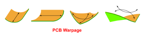
In the realm of pcb assembly, several challenges can arise that may hinder the efficiency and effectiveness of the assembly process. One common issue is ensuring the precise alignment of components on the printed circuit board (PCB), which is crucial for a successful PCBA. Misalignment can lead to electrical failures or short circuits, so utilizing specialized tools like pick-and-place machines can greatly mitigate this issue. Another challenge involves soldering defects such as cold joints or solder bridging, which can compromise circuit connectivity. To combat this, employing proper soldering techniques and using quality solder materials is essential. Additionally, managing component variations, including size and footprint differences, requires a keen understanding of design specifications; thus, thorough documentation and careful oversight during assembly are vital.
Temperature control during the soldering process is yet another challenge faced in pcb assembly. If temperatures are too high or too low, they can adversely affect solder quality and joint reliability. Implementing temperature profiling for reflow ovens or using thermocouples during hand soldering can help maintain optimal conditions. Lastly, achieving consistent quality across multiple boards often proves difficult without rigorous quality control measures in place. Regular inspections and automated testing systems ensure that defects are identified early, allowing for corrective actions before the PCBA reaches the final customer. By addressing these challenges head-on with informed strategies and appropriate tools, professionals can enhance their PCB assembly outcomes significantly.
Quality Control: Ensuring a Flawless Assembly Process
In the realm of pcb assembly, maintaining high standards through quality control is essential for achieving reliable and efficient results. The process of quality assurance in pcba involves a series of systematic practices designed to identify and mitigate potential defects at various stages of assembly. Implementing rigorous inspection protocols ensures that every component is up to industry standards, significantly reducing the likelihood of electronic failure in the final product. Utilizing tools such as Automated Optical Inspection (AOI) and X-ray inspection, engineers can accurately assess solder joints and component placements, making it easier to spot issues early. Furthermore, conducting thorough testing throughout the assembly process – including functional testing and environmental stress tests – provides valuable insights into the quality of the pcb assembly. By fostering a culture of continuous improvement and adherence to best practices, organizations not only enhance their production quality but also build customer trust in their electronic solutions. Effective quality control ultimately leads to fewer returns, increased operational efficiency, and a strong reputation in the competitive landscape of electronics manufacturing.
Advanced Techniques for Complex PCB Designs
When tackling pcb assembly for intricate designs, advanced techniques become essential to ensure high-quality results. One such technique involves the use of multi-layer boards, which allow for greater functionality but require precise alignment during assembly. To achieve this, utilizing a robust solder paste application method can greatly enhance the precision of component placement. Additionally, employing laser-cut stencils helps streamline the process by ensuring correct paste deposition in complex geometries.
It’s also crucial to consider the thermal management aspect of pcba, as densely packed components can lead to overheating if not designed effectively. Integrating thermal vias and copper pours into your design can facilitate effective heat dissipation while maintaining a compact structure. Furthermore, incorporating technologies like via-in-pad and blind via connections will optimize space and improve electrical performance.
Integrating advanced inspection methods such as Automated Optical Inspection (AOI) and X-ray imaging further ensures that every joint is secure and functional, especially in high-density areas. These practices are not only instrumental in enhancing quality control but also serve to identify potential issues early in the assembly process, saving time and resources.
In summary, mastering these advanced techniques is pivotal for those involved in complex pcb assembly projects, whether you’re a seasoned professional or just starting out in the world of electronics design and assembly. The right combination of methods ensures that your pcba stands up to performance expectations while minimizing errors and maximizing efficiency.
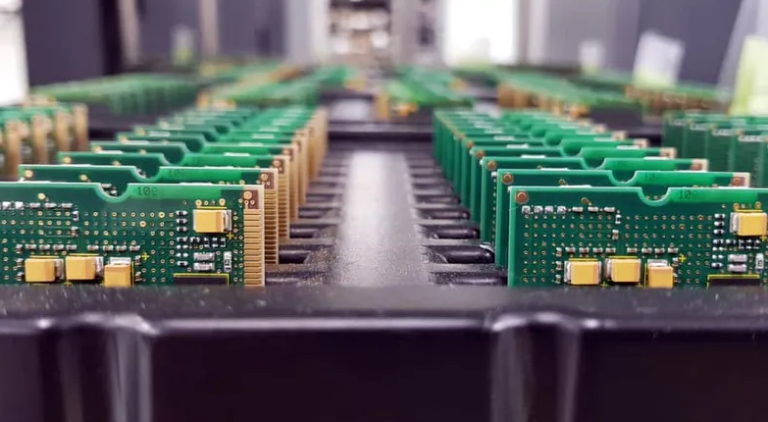
Exploring Automated vs. Manual Assembly Methods
In the field of pcb assembly, the choice between automated and manual assembly methods plays a critical role in determining the efficiency and quality of the final product. Automated assembly employs sophisticated machinery and robots to perform repetitive tasks with high precision, making it an ideal choice for large-scale production. This approach significantly reduces human error and increases throughput, making it a preferred option for many manufacturers focusing on consistent quality in their printed circuit board assembly (PCBA) processes. Conversely, manual assembly shines in settings that require a high degree of customization or small batch sizes. Skilled technicians can easily adapt to unique designs and rectify issues on the fly, which can sometimes be a challenge for automated systems that may struggle with varied or complex layouts. Additionally, manual methods often offer a more hands-on approach, allowing for meticulous inspection during the process that can enhance final product integrity. Ultimately, the decision between automated and manual methods in pcb assembly relies on factors such as volume requirements, cost considerations, and specific project needs, highlighting the importance of strategically evaluating each method’s advantages in relation to project goals.
Future Trends in PCB Assembly Technology
The future of PCB assembly technology is poised for remarkable transformation, driven by advancements in automation and artificial intelligence. As industries continue to demand higher efficiency and reliability, pcba processes are evolving to incorporate innovative technologies such as robotics and machine learning. These developments are not only speeding up the assembly line but also enhancing precision, reducing defects significantly. Furthermore, the integration of smart manufacturing principles is transforming traditional pcb assembly into a more interconnected and intelligent process, enabling real-time monitoring and data analytics that help in maintaining quality standards. Another trend is the growing emphasis on sustainability; manufacturers are increasingly adopting eco-friendly materials and processes to minimize waste while ensuring high performance of their products. As a result, the landscape of pcb assembly is expanding to include next-gen techniques such as 3D printing and flexible circuits, which promise increased versatility for complex designs. Embracing these innovative solutions will be crucial for professionals seeking to stay ahead in an ever-competitive market, making it imperative to continually adapt and integrate these emerging technologies into their workflows.
Conclusion
Achieving success in PCB assembly requires a comprehensive understanding of both the design principles and the practical assembly techniques involved in the process. By exploring various methodologies, tools, and materials needed for PCBA, individuals can enhance their skills significantly. Whether you’re a beginner or an experienced professional, embracing a structured approach to the assembly process can help mitigate common challenges. Furthermore, integrating quality control measures ensures that each project meets or exceeds industry standards, resulting in a flawless outcome. As technology continues to advance, keeping an eye on the future trends in PCB assembly technology—such as automation and innovative materials—will provide valuable insights and strategies for ongoing improvement in your projects. Ultimately, mastering board PCB assembly not only contributes to personal growth but also fosters success in the broader landscape of electronics engineering.
FAQs
What is PCB assembly?
PCB assembly, or PCBA, is the process of connecting electronic components to a printed circuit board (PCB) to create a functional electronic circuit.
What are the main steps involved in PCB assembly?
The main steps in PCB assembly include designing the PCB, sourcing components, soldering the components onto the PCB, and performing testing and quality checks to ensure functionality.
How can I ensure quality during PCB assembly?
To ensure quality in PCBA, implement quality control measures such as visual inspection, component placement verification, and functional testing at various stages of the assembly process.
What tools do I need for manual PCB assembly?
Essential tools for manual PCB assembly include soldering irons, tweezers, magnifying lamps, multimeters for testing, and cleaning supplies to maintain a clean working area.
What challenges can arise during PCB assembly?
Common challenges in PCBA include component misplacement, solder bridging, insufficient solder joints, and managing heat sensitivity of certain components. Each of these issues requires specific strategies to resolve.
For a deeper understanding of board PCB assembly techniques and resources, please visit this link for more information.