Mastering Complex PCB Assembly: Techniques for Success
Key Takeaways
Mastering complex PCB assembly (PCBA) involves a systematic approach that emphasizes understanding foundational principles, utilizing the right tools, and implementing advanced techniques. Successful PCB assembly begins with a comprehensive grasp of the basics—familiarity with components, circuit design, and assembly processes lays the groundwork for more complicated tasks. The selection of high-quality tools and equipment is essential for any complex PCB project, as they significantly influence both the efficiency and precision of your work. Incorporating advanced techniques such as surface mount technology (SMT), automated assembly processes, and effective layout designs can streamline your operations, reducing both time and costs.
Moreover, adhering to best practices for ensuring precision is vital; this includes meticulous attention to detail in design specifications, thorough documentation, and systematic review processes. It’s equally important to actively troubleshoot common issues that arise throughout the PCB assembly process—problems like misaligned components or soldering defects can derail projects if not addressed swiftly. Finally, the significance of testing and verification cannot be overstated; robust testing routines ensure that every PCBA meets design requirements and functions as intended. As you navigate through ongoing advancements and future trends in complex PCB assembly, staying informed will empower you to adapt strategies that optimize outcomes in your projects effectively.
Understanding the Basics of PCB Assembly
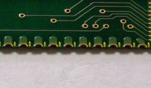
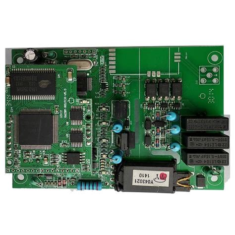
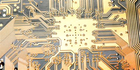
Printed Circuit Board (PCB) assembly is a crucial step in the manufacturing of electronic devices, where various components are soldered onto a pre-defined board layout, forming a functional circuit. The complexity of PCB assembly can vary significantly based on the design and functionality of the circuit. Understanding these fundamentals is essential for anyone involved in pcba projects. A solid grounding in the basic components, such as resistors, capacitors, and integrated circuits, is paramount. Knowledge of different types of assemblies—ranging from surface mount technology (SMT) to through-hole technology—ensures that practitioners can choose suitable methods for their requirements.
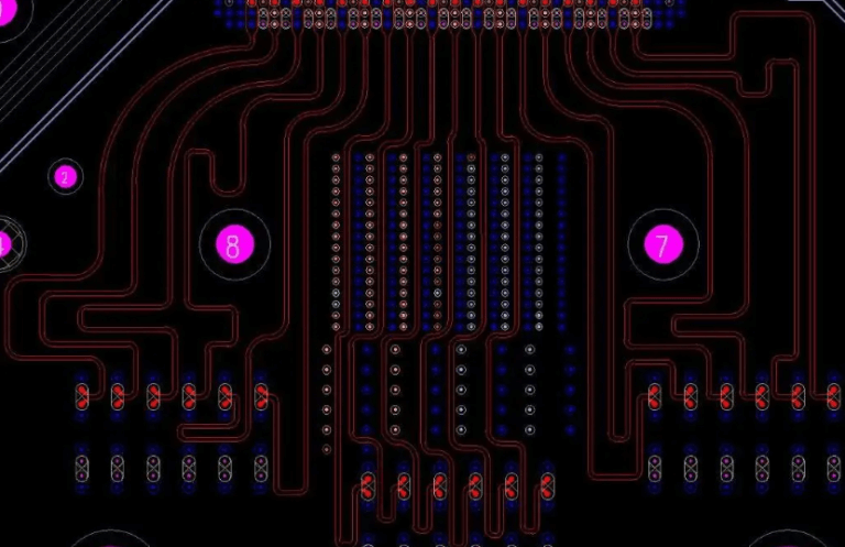
One pivotal factor to consider during pcb assembly is the layout design, which directly affects performance and manufacturing efficiency. Moreover, keeping track of component tolerances and adhering strictly to placement guidelines enhances reliability in both performance and durability. Ultimately, every successful project hinges on having a clear grasp of these basic principles.
| Component Type | Description | Common Uses |
|---|---|---|
| Resistors | Control current flow | Voltage dividers |
| Capacitors | Store electrical energy | Smoothing voltage fluctuations |
| Integrated Circuits | Packaged circuit components | Microcontrollers |
| Inductors | Store energy in a magnetic field | Filtering applications |
“A meticulous approach to understanding component functionality can significantly elevate the quality of your final product.”
Incorporating solid foundational knowledge into your workflow allows for strategic planning when tackling more complex aspects like soldering techniques or managing thermal issues during assembly. By mastering these basics, you set yourself up for success as you move deeper into advanced methods and innovative practices in pcb assembly projects.
Tools and Equipment Essential for Complex PCB Projects
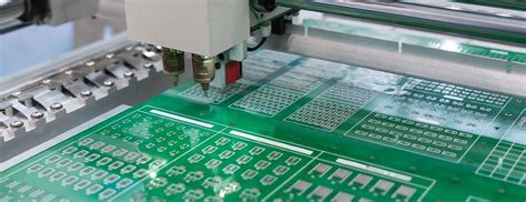
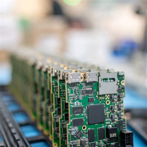
In the world of PCB assembly (PCBA), having the right tools and equipment is crucial to achieving high-quality results. A solid understanding of both manual and automated techniques can significantly impact the overall outcome of your projects. Essential tools include precision soldering irons, which allow for controlled heat application, ensuring that components are securely attached without damaging sensitive parts. Additionally, pick-and-place machines offer efficiency in handling multiple components at once, reducing labor time in complex designs.
Moreover, the use of oscilloscopes and multimeters provides real-time testing capabilities to verify circuit functions during the assembly process. These devices are invaluable for diagnosing issues early, ultimately saving time and resources. High-quality PCB fabrication software is also critical for designing layouts that maximize space while minimizing errors—a common challenge in complex PCBA scenarios.
For final quality checks, implementing a robust inspection system with automated optical inspection (AOI) technology can detect defects that may go unnoticed by the human eye. This equipment not only enhances efficiency but also ensures precision in every step of PCB assembly, enabling smoother pathways to successful project completions. By prioritizing these essential tools and equipment, you set a strong foundation for any complex PCB project.
Advanced Techniques for Efficient PCB Assembly
When navigating the intricacies of PCB assembly, employing advanced techniques is vital for achieving high-quality results in your projects. One effective approach involves automating processes through the integration of robotics and sophisticated machinery. This not only increases speed but also minimizes the risk of human error, enhancing overall efficiency. Furthermore, utilizing advanced placement technologies can significantly improve the accuracy of component positioning, which is crucial in complex assemblies where space is at a premium.
Implementing layered assembly techniques allows engineers to tackle complexity by breaking down a project into manageable parts, facilitating easier troubleshooting and modification as necessary. Additionally, leveraging data analytics and monitoring during assembly can provide real-time insights, ensuring that any anomalies are detected and addressed immediately.
Adopting best practices such as standardized documentation and maintaining clear communication among team members enhances coherence throughout the assembly process. These practices not only streamline production but also foster collaborative problem-solving, which is essential when facing challenges in PCBA projects.
To summarize, optimizing efficiency in PCB assembly hinges on embracing a combination of innovative technologies and sound methodologies that enhance precision while reducing lead times and costs. By continually refining these advanced techniques, organizations can remain competitive in an ever-evolving landscape, ensuring successful outcomes for their complex PCB endeavors.
Best Practices for Ensuring Precision in PCB Design
Achieving precision in PCB assembly is crucial for the functionality and reliability of electronic devices. To start, the design phase should be approached with meticulous attention to detail. Utilizing advanced design software that includes features like real-time error checking and design rule checks can significantly reduce mistakes that might lead to faults in the final product. Proper footprint selection is also vital; ensuring that each component’s footprint accurately matches its specifications can prevent alignment issues during assembly. Additionally, implementing a thorough review process involving multiple sets of eyes can catch errors early, thus enhancing the overall quality of your PCBA.
Another key practice is to organize the workspace effectively by ensuring that tools are readily available and components are clearly labeled. This not only speeds up the process but also minimizes the chances of using incorrect components, which could lead to poor performance or failure. Moreover, employing techniques like pair programming when designing PCBs can facilitate immediate feedback and reduce missteps. Regularly updating your skills and knowledge about emerging trends and technologies related to complex PCB assembly will further bolster your precision efforts.
By paying attention to these best practices, engineers can foster an environment where precision prevails, ultimately leading to more reliable products when it comes time for mass production or prototyping in any PCB project.
Troubleshooting Common Issues in PCB Assembly
In the intricate world of PCB assembly (PCBA), issues can arise at any stage of the process, leading to potential setbacks in project timelines and overall efficiency. One of the most common problems encountered is misalignment of components during the placement phase. This can be attributed to inadequate alignment tools or poor handling practices. To mitigate this, employing automated placement machines and ensuring precise calibration before running production runs is essential. Another frequent challenge is soldering defects such as cold joints or bridges. These can occur due to improper solder paste application or suboptimal temperatures during the soldering process. Utilizing a stencil printing technique that ensures uniform paste distribution combined with precise temperature controls during reflow can significantly reduce these issues.
Moreover, environmental factors such as dust and humidity can adversely affect PCBA quality. It is crucial to maintain a clean working environment, using suitable filters and dehumidifiers in PCB assembly areas to prevent contamination that could lead to failures down the line. Conducting thorough inspections at every stage—be it through visual checks or employing automated optical inspection (AOI) systems—can catch these problems before they escalate into more significant barriers, reinforcing the importance of a proactive approach in ensuring device reliability and operational success.
In summary, efficient troubleshooting requires both understanding common pitfalls and implementing advanced strategies and tools tailored for complex PCB assembly, which ultimately will drive projects toward optimal success while enhancing precision along the way.
The Importance of Testing and Verification in PCB Projects
In any PCB assembly process, especially for complex PCB projects, thorough testing and verification is imperative to achieving reliable outcomes. The intricacies of PCBA increase the risk of errors, making it essential to adopt rigorous verification protocols at various stages of production. Not only does this help identify potential issues early, but it also ensures that the final product meets all required specifications and functions as intended. Techniques such as automated optical inspection (AOI), functional testing, and in-circuit testing (ICT) are crucial for verifying the integrity of the assembled boards. These methods allow for the detection of defects such as soldering issues, component misalignment, or signal integrity problems, which could compromise functionality. Therefore, implementing a robust testing strategy not only enhances quality but also minimizes rework, ultimately leading to reduced costs and improved time-to-market for your PCB assembly endeavors. In summary, prioritizing testing and verification in your PCBA workflow is vital for ensuring high-quality results and long-term success in electronic manufacturing projects.
Future Trends in Complex PCB Assembly Techniques
The landscape of pcba is constantly evolving, influenced by advancements in technology and the demands of modern electronics. One of the most notable trends in complex PCB assembly is the increasing integration of automation and robotics. Automated processes significantly enhance efficiency, reduce labor costs, and minimize human error. Coupled with this is the rise of smart manufacturing, where IoT (Internet of Things) devices collect data throughout the pcb assembly process, allowing for real-time monitoring and adjustments to optimize production.
Another key trend is the adoption of multilayer PCBs, which enable more complex designs in a smaller footprint. This development meets the demand for compact electronic devices without sacrificing performance. Furthermore, advancements in materials science have led to the use of alternative substrates that offer improved thermal management and signal integrity, catering to high-frequency applications.
As technological demands grow, techniques such as surface mount technology (SMT) are evolving to accommodate finer pitches and smaller components. This raises the need for new soldering technologies like laser soldering, which provides precision while preserving the integrity of sensitive components.
Lastly, emphasis on sustainability is becoming a driving force in pcb assembly practices, encouraging manufacturers to adopt eco-friendly materials and processes. The trend towards minimizing waste and energy consumption aligns with global initiatives for sustainable manufacturing.
In conclusion, staying ahead in complex PCB assembly techniques not only involves embracing these trends but also adapting strategically to incorporate them into existing workflows for optimal success.
Conclusion
In the realm of PCB assembly, mastering complex projects requires a deep understanding of various techniques and methodologies that enhance both efficiency and precision. Throughout this article, we have explored essential components that contribute to successful PCBA processes, from the fundamental principles during the initial stages to advanced techniques that can save time and resources. Utilizing appropriate tools and equipment can lead to significant improvements in assembly accuracy, ultimately resulting in higher-quality electronic products. Moreover, implementing best practices for design and testing plays a pivotal role in mitigating potential issues during assembly. As technology continues to evolve, staying abreast of future trends in complex PCB assembly will empower engineers and technicians to further refine their skillsets, ensuring they remain competitive in an ever-advancing industry. By focusing on the techniques discussed, professionals can enhance their workflows and deliver superior outcomes in all PCB assembly endeavors.
FAQs
What is PCB assembly?
PCB assembly, or PCBA, is the process of soldering electronic components onto a printed circuit board (PCB) to create functional electronic devices. This involves a series of steps including component placement, soldering, and testing.
What are the main steps involved in PCBA?
The main steps in PCB assembly include design preparation, component procurement, solder paste application, placement of components, soldering (either reflow or wave), inspection, and testing to ensure functionality.
How can I ensure precision in my PCB assembly projects?
To ensure precision in your PCBA, implement best practices such as using high-quality components, maintaining a clean workspace, utilizing automated placement machines where possible, and conducting thorough inspections at every stage of the assembly process.
What tools are essential for complex PCB projects?
Essential tools for complex PCB assembly include soldering stations, stencil printers for applying solder paste, pick-and-place machines for component placement, and inspection tools like microscopes or X-ray systems for checking solder joints.
Why is testing important in PCB assembly?
Testing is crucial in PCB assembly as it helps identify defects or faults early in the process. Proper testing ensures that the final product meets quality standards and performs correctly under various conditions.