Mastering Double Layer PCB Manufacturing: A Complete Guide
Key Takeaways
In mastering double layer PCB manufacturing, there are several key aspects that you should keep in mind. First, understanding the fundamental characteristics of double layer PCBs will lead you to appreciate their advantages, such as increased design flexibility and reduced overall pcb manufacturing cost. A significant part of your journey involves considering design parameters. By ensuring that your designs are optimized for a two-layer configuration, you can significantly enhance the performance of the final product.
Moreover, you must choose materials wisely; high-quality substrates and conductive materials are essential for robust performance, influencing your decisions when collaborating with various pcb manufacturing companies. As you navigate through the processes involved in pcb manufacturing, being aware of the sequential steps—from material selection to fabrication—will enhance your ability to achieve high quality and efficiency in production.
Additionally, acknowledging common challenges within the pcb manufacturing business landscape is crucial. Solutions often require proactive methods, ensuring that your double layer PCBs meet industry standards while maintaining competitive pricing in the market. By synthesizing this knowledge, you position yourself better within an ever-evolving industry landscape, opening doors to diverse applications that utilize these critical technologies.
Understanding Double Layer PCBs: Key Features and Benefits
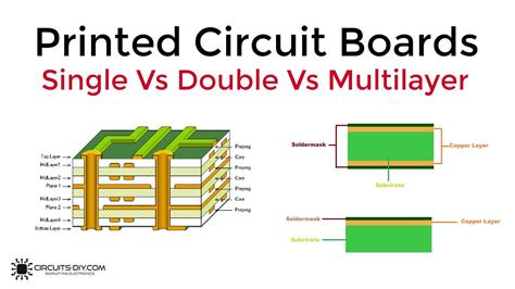
In the realm of PCB manufacturing, double layer PCBs stand out due to their unique combination of functionality and compactness. These boards typically feature two layers of conductive material, which allows for more complex circuit designs compared to single-layer options. The ability to have conductive pathways on both sides of the board not only enhances design flexibility but also helps in reducing the overall size and weight of devices, making them ideal for applications where space is at a premium. For those interested in the PCB manufacturing business, it is vital to recognize that double layer PCBs can often offer increased reliability and performance due to better signal integrity and reduced electromagnetic interference. Moreover, understanding the PCB manufacturing cost is essential; although they may be more expensive than their single-layer counterparts, the benefits often justify this investment for many applications. As you delve deeper into your projects or collaborations with various PCB manufacturing companies, you will find that these boards serve a wide range of industries, including telecommunications, automotive, and consumer electronics, thanks to their durability and efficiency.
Design Considerations for Double Layer PCB Layout
When embarking on double layer PCB manufacturing, one of the most critical aspects to pay attention to is the layout design. Your design needs to accommodate not only the physical component placements but also the electrical performance required for your application. Begin with a clear understanding of how components interact on the board; optimizing trace routing is essential for signal integrity and minimizing noise. It’s crucial to consider factors such as layer stacking, power distribution, and ground planes when drafting your layout. Choosing the right pcb manufacturing company can greatly influence your design’s success, as their capabilities will dictate what designs can be effectively realized.
Another vital consideration involves layer thickness and spacing, which affect the overall pcb manufacturing cost. Keep in mind that deviations from standard designs may incur additional costs, so aim for a balance between innovative design and practicality. You should also ensure that your layout meets any specific industry standards that apply, which often necessitate additional documentation and testing.
“Effective layout design is an investment that pays off in performance and reliability.”
Ultimately, by meticulously addressing these design elements, you set a solid foundation for smooth operations in double layer PCB manufacturing, paving the way for high-quality products suited to diverse applications. Remember, a well-thought-out layout not only enhances performance but can also ease the fabrication process, making it more cost-effective when working with any pcb manufacturing business. Whether you are developing consumer electronics or industrial applications, prioritizing these considerations will contribute significantly to producing reliable and efficient double layer PCBs. For more insights and specialized services in this field, check out resources from Andwin PCB.
Choosing the Right Materials for Double Layer PCB Production
Selecting the appropriate materials for double layer PCB production is crucial for ensuring optimal performance and reliability. The materials you choose directly affect not only the pcb manufacturing cost but also the overall durability and functionality of the final product. For instance, copper is typically used as the conductive layer due to its excellent electrical conductivity and thermal properties. When considering pcb manufacturing companies, it’s essential to inquire about their sourcing of materials, as high-quality copper will enhance your device’s performance.
In addition to copper, substrates such as FR-4 (a fiberglass epoxy) are commonly used for its balance of cost-effectiveness and electrical performance. FR-4’s dielectric properties make it a go-to choice for many PCB applications. It’s also important to evaluate other materials like polyimid or ceramic, particularly when dealing with high-temperature or specialized applications, influencing your pcb manufacturing business decisions.
Here’s a quick comparison of suggested materials:
| Material | Characteristics | Cost Factor | Common Applications |
|---|---|---|---|
| Copper | Excellent conductivity, flexible | Moderate | General-purpose electronics |
| FR-4 | Good balance; versatile | Low | Consumer electronics |
| Polyimid | High heat resistance | Higher | Aerospace, medical equipment |
| Ceramic | Excellent dielectric properties | Higher | Specialized high-frequency uses |
When engaging with potential pcb manufacturing companies, ensure you ask about the specifications of their chosen materials. This knowledge not only informs you about potential performance outcomes but also impacts long-term operational costs within your products. The right material selection can significantly enhance reliability while minimizing risks associated with corrosion or thermal instability during operation. Adapt your choices based on your application needs while keeping an eye on both immediate costs and long-term benefits.
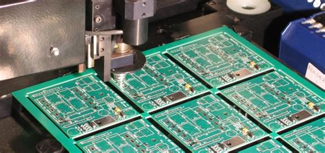
Step-by-Step Process of Double Layer PCB Manufacturing
The pcb manufacturing process for double layer PCBs involves several critical stages, each contributing to the overall performance and reliability of the final product. Firstly, you need to create a detailed design layout, ensuring that both layers are efficiently utilized to meet your circuit requirements. This step often requires specialized software that helps in organizing your components and routing traces effectively. Next comes the preparation of materials; you will select suitable substrates and copper sheets, considering aspects such as dielectric properties and thermal conductivity.
Once the materials are ready, begin the manufacturing process by etching the copper layers, which involves applying a photoresist material onto the copper surface, exposing it to UV light to create patterns that will define your circuitry. After developing these patterns, you will proceed to etch away unwanted copper using a chemical solution, which leaves behind only the necessary circuitry.
Following this, layers need to be laminated together using heat and pressure to ensure a strong bond between them. This step is essential in maintaining circuit integrity during operation. After lamination, drilling holes for vias—connections between layers—becomes crucial; precise drilling ensures that electrical signals can flow seamlessly across both layers.
The final steps include applying solder mask and silkscreen layers before cutting the PCB to its final shape. Throughout this entire process, quality control is vital; ensuring that each stage adheres to industry standards can significantly impact your pcb manufacturing cost and overall success in the pcb manufacturing business sector. By following these steps meticulously, you can create efficient double layer PCBs suitable for various applications across multiple industries.
Quality Control in Double Layer PCB Fabrication
Quality control in double layer PCB fabrication is a critical component that ensures the reliability and efficiency of the final product. This process begins with rigorous testing of raw materials, which are essential in maintaining high standards throughout the PCB manufacturing journey. You should prioritize sourcing components from reputable PCB manufacturing companies that adhere to industry regulations and quality benchmarks. The importance of meticulous inspection cannot be overstated; you will find that implementing a robust quality control system minimizes production flaws, thereby reducing long-term PCB manufacturing costs.
During the production process, continual monitoring is implemented to detect any discrepancies. You should be aware that factors such as temperature fluctuations and humidity can impact the integrity of your boards, which is why maintaining a controlled environment during fabrication is vital. Employing automated testing methods, such as Automated Optical Inspection (AOI), allows for immediate feedback on the quality of your boards, making it easier to identify defects early on.
For those engaged in the PCB manufacturing business, adopting a proactive approach to quality control not only enhances product consistency but also boosts customer satisfaction. Keeping thorough documentation of inspection processes also helps in ensuring compliance with international standards, thus positioning your business competitively in an ever-evolving market.
In summary, paying close attention to quality control can dramatically influence both the outcome of your production efforts and your long-term success within the industry. By investing time and resources into maintaining high-quality standards, you set yourself up for a reputation built on reliability and excellence in double layer PCB fabrication.
Applications and Industries Utilizing Double Layer PCBs
Double layer PCBs play a pivotal role across numerous industries, considerably enhancing the functionality of electronic devices. In the realm of consumer electronics, double layer PCB manufacturing is essential for devices like smartphones and tablets, where space is limited but performance requirements are high. The compact design offered by double layer PCBs allows for efficient routing of electrical signals while maintaining a low pcb manufacturing cost, making them an ideal choice for mass production.
In automotive applications, double layer PCBs are utilized in advanced driver-assistance systems (ADAS) and infotainment systems, where reliability and robustness are critical. The complex circuitry involved in these systems benefits greatly from the efficiency of PCB manufacturing companies, which can design and produce boards capable of withstanding harsh environmental conditions.
The medical industry also heavily relies on double layer PCB manufacturing, as devices like patient monitoring systems and diagnostic equipment require high levels of precision and reliability. Here, the emphasis is on creating durable boards that meet strict regulatory standards while keeping costs manageable.
Additionally, the telecommunications sector utilizes these versatile boards to support a wide range of applications from network equipment to wireless communication devices. The demand for efficient data transmission drives innovation in pcb manufacturing business, leading to advancements in board design that facilitate increased functionality while minimizing space.
By understanding these applications, you can appreciate the vital role double layer PCBs play in modern technology and their impact across different sectors. Whether you are exploring opportunities in pcb manufacturing or seeking to enhance your existing projects, recognizing where double layer PCBs fit into your strategy is essential for success.
Common Challenges in Double Layer PCB Manufacturing and Solutions
In the world of double layer PCB manufacturing, there are several challenges that you may encounter. One of the most common issues is achieving proper alignment during the pcb manufacturing process. Misalignment can lead to short circuits or open connections, which are detrimental to the functionality of your final product. To combat this, utilizing advanced imaging techniques and ensuring a robust design verification process is crucial; PCB manufacturing companies often recommend incorporating automated alignment systems to enhance precision.
Another challenge is managing the pcb manufacturing cost effectively. It can escalate due to the intricacies involved in designing and fabricating double layer PCBs, particularly if high-quality materials or specialized features are required. However, opting for bulk production or negotiating pricing with different pcb manufacturing companies can help you streamline your expenses while maintaining quality.
Thermal management is also a critical concern that must be addressed during development. Heat dissipation in double layer PCBs requires careful consideration of materials and layout design to prevent overheating, which can lead to failures. Implementing thermal simulations in your design phase can significantly aid in identifying potential issues before production begins.
Lastly, achieving reliability through quality control measures is vital. Regular inspections during each stage of the pcb manufacturing business not only ensure compliance with standard specifications but also help identify defects early on. Collaborating with reputable manufacturers who adhere to international quality standards will further mitigate risks and enhance overall product integrity. By addressing these challenges effectively, you can enhance the efficiency and reliability of your double layer PCB products.
Conclusion
In summary, successful double layer PCB manufacturing hinges on understanding various elements that impact the overall PCB manufacturing cost. By ensuring that you choose the right materials and adhere to precise design considerations, you not only optimize production efficiency but also enhance the reliability of the final product. It is important to realize that partnering with reputable PCB manufacturing companies can make a significant difference in quality and lead times. Furthermore, recognizing common challenges in the PCB manufacturing business, such as troubleshooting design errors or ensuring quality control, allows you to proactively address these issues and streamline your production process. Ultimately, mastering the intricacies of double layer PCB production can lead to substantial benefits across multiple applications and industries, making your products more competitive in an ever-evolving market.
FAQs
What is double layer PCB manufacturing?
Double layer PCB manufacturing refers to the process of creating printed circuit boards with two conductive layers. This type of design allows for more complex circuit layouts, enabling greater functionality in a compact form factor.
What materials are typically used in double layer PCB production?
The choice of materials in double layer PCB production is crucial. Common materials include FR-4, which is a glass-reinforced epoxy laminate, and various copper thicknesses that cater to different electrical requirements. Understanding material properties ensures the reliability of the PCB throughout its lifecycle.
How can I evaluate the costs associated with double layer PCB manufacturing?
The PCB manufacturing cost can vary based on factors such as design complexity, material selection, and production scale. Engaging with multiple PCB manufacturing companies allows you to compare quotes and find competitive pricing while ensuring quality.
What are common applications for double layer PCBs?
Double layer PCBs are utilized across various industries, including consumer electronics, automotive systems, and telecommunications. Their versatility makes them ideal for applications that require efficient space utilization while delivering high performance.
How do I choose a reliable PCB manufacturing business?
When selecting a PCB manufacturing business, consider their reputation, customer reviews, production capabilities, and quality control processes. A reliable partner will help you navigate the intricacies of pcb manufacturing, ultimately leading to a successful project outcome.