Mastering Key Manufacturing Insights for Multi Layer PCB Assembly

Key Takeaways
Successful multi-layer PCB assembly relies on understanding critical factors that govern design, material compatibility, and process precision. PCBA (Printed Circuit Board Assembly) efficiency begins with meticulous design validation, where layer stack-up configurations and impedance matching are optimized to prevent signal degradation. Material selection—particularly high-Tg laminates and low-loss dielectrics—directly impacts thermal stability and electrical performance during PCB assembly.
Equally vital is mastering lamination process controls, including temperature gradients and pressure uniformity, to eliminate delamination risks in multi-layer structures. Advanced quality assurance protocols, such as automated optical inspection (AOI) and X-ray testing, ensure defect-free interconnects across layers. Transitioning to PCBA, engineers must balance thermal management strategies—like embedded copper cores—with signal integrity requirements to maintain reliability in high-density layouts.
By integrating these insights, manufacturers can reduce rework cycles, enhance yield rates, and meet stringent performance benchmarks for complex multi-layer PCB assembly projects.
Multi-Layer PCB Design Best Practices
Effective multi-layer PCB assembly begins with meticulous design strategies that balance electrical performance and manufacturability. A well-planned layer stackup configuration is critical, ensuring optimal signal routing while minimizing electromagnetic interference (EMI). Designers must prioritize impedance control by aligning trace widths and dielectric materials with target specifications, particularly for high-speed circuits. Proper power and ground plane allocation reduces noise and stabilizes voltage distribution, which is essential for complex PCBA applications.
To enhance reliability, incorporate thermal relief pads and via-in-pad techniques to manage heat dissipation during soldering processes. Component placement should adhere to design for manufacturing (DFM) guidelines, maintaining adequate spacing for automated assembly equipment. Additionally, integrating test points and fiducial markers streamlines quality inspections post-PCB assembly.
Collaboration between design and manufacturing teams ensures alignment on material choices, such as high-glass transition temperature (Tg) substrates, which improve thermal resilience. By addressing these factors early, designers mitigate risks in later stages, ensuring seamless transitions to lamination and PCBA processes. This holistic approach not only accelerates production but also elevates the functional integrity of multi-layer boards.
Critical Material Selection Factors Explained
Selecting appropriate materials is foundational to successful multi-layer PCB assembly, directly influencing performance, durability, and cost-efficiency. Key considerations include the thermal stability of substrates, copper foil thickness, and the compatibility of dielectric materials with high-frequency applications. For instance, FR-4 remains a popular choice for general-purpose PCBA, but advanced applications may require polyimide or ceramic-filled laminates to withstand extreme temperatures or signal loss reduction.
The table below highlights critical material properties and their impact on PCB assembly outcomes:
| Material Property | Impact on Assembly | Common Options |
|---|---|---|
| Glass Transition (Tg) | Determines heat resistance | FR-4 (Tg 130–180°C), Polyimide (Tg >250°C) |
| Dielectric Constant (Dk) | Affects signal integrity | Rogers RO4000®, Isola IS410 |
| Copper Weight | Influences current-carrying capacity | 0.5 oz, 1 oz, 2 oz |
Additionally, solder mask selection must balance adhesion strength and chemical resistance to prevent delamination during PCBA processes. For multi-layer designs, mismatched coefficients of thermal expansion (CTE) between layers can lead to warping or cracking, emphasizing the need for harmonized material stacks. Environmental factors, such as moisture absorption rates, further dictate reliability in humid operating conditions. By aligning material choices with design requirements and manufacturing workflows, engineers mitigate risks while optimizing multi-layer PCB assembly efficiency.
Lamination Process Control Techniques Unveiled
Effective multi-layer PCB assembly relies on precise control of the lamination process, where alternating layers of conductive and insulating materials are bonded under heat and pressure. Achieving optimal thermal stability and void-free bonding requires strict management of temperature gradients, pressure distribution, and dwell time during curing. For instance, maintaining a balanced pressure profile across the panel prevents delamination, while calibrated heating rates minimize resin flow inconsistencies.
Tip: Implement real-time monitoring systems to track press-plate parallelism and temperature uniformity during lamination—critical for ensuring consistent layer alignment in high-density PCBA designs.
Material selection also plays a pivotal role. Prepregs with controlled resin content (e.g., low-flow vs. high-flow formulations) must align with the layer stackup’s glass transition temperature (Tg) requirements. Post-lamination, advanced techniques like cross-sectional analysis and thermal stress testing validate interlayer adhesion integrity, reducing defects in subsequent PCB assembly stages. By integrating these controls, manufacturers enhance yield rates and long-term reliability in complex multi-layer PCBA applications.
Advanced Quality Assurance Testing Methods
Ensuring reliability in multi-layer PCB assembly demands rigorous quality assurance testing protocols. Modern PCBA workflows integrate automated optical inspection (AOI) to detect soldering defects, misaligned components, or trace inconsistencies across densely packed layers. For internal layer validation, X-ray inspection becomes indispensable, particularly for identifying voids in via fillings or delamination risks introduced during high-pressure lamination cycles.
In-circuit testing (ICT) verifies electrical performance by simulating operational conditions, ensuring signal integrity aligns with design specifications. Additionally, thermal cycling tests expose boards to extreme temperature fluctuations, validating material resilience and solder joint durability — critical for applications in automotive or aerospace systems.
Advanced labs now employ boundary-scan testing to diagnose interlayer connectivity issues without physical probes, minimizing mechanical stress on delicate traces. To align with PCB assembly efficiency goals, statistical process control (SPC) tools analyze production data in real time, flagging deviations in parameters like dielectric thickness or copper plating uniformity.
These methodologies not only reduce field failure rates but also complement upstream processes, such as material selection and lamination controls, creating a闭环 quality ecosystem. By integrating these tests, manufacturers ensure PCBA outputs meet both functional benchmarks and long-term reliability expectations.
Thermal Management Strategies for PCBs
Effective thermal management is critical in multi-layer PCB assembly to ensure long-term reliability and prevent performance degradation. As component density increases in modern PCBA designs, heat dissipation challenges intensify, requiring strategic planning during both design and manufacturing phases. One foundational approach involves optimizing copper distribution and thermal via placement to create efficient heat pathways. For high-power applications, integrating metal-core substrates or embedded heat sinks can significantly reduce hot spots.
Material selection plays a pivotal role, with high-Tg (glass transition temperature) laminates and thermally conductive prepregs enhancing resistance to thermal stress. Advanced PCB assembly workflows often incorporate simulation tools to model heat distribution patterns before prototyping, minimizing iterative costs. Additionally, selective use of thermal interface materials (TIMs) between layers improves heat transfer efficiency during the lamination process.
In automated PCBA lines, real-time thermal monitoring systems enable adjustments to soldering profiles, preventing warping or delamination. For mission-critical applications, combining passive strategies—such as optimized trace routing—with active cooling solutions like micro-fans or heat pipes ensures balanced thermal performance. These measures not only extend product lifespan but also align with broader quality control frameworks outlined in earlier sections, reinforcing the interdependence of design, material science, and manufacturing precision.
Signal Integrity Optimization Essentials Guide
Achieving optimal signal integrity in multi-layer PCB assembly requires balancing design precision and material performance. Impedance control remains foundational, demanding careful alignment of trace widths, dielectric thickness, and substrate materials to minimize reflections. For high-speed PCBA, selecting low-loss laminates like Rogers 4350B or Isola FR408 reduces signal attenuation, particularly in layers carrying GHz-frequency traces.
Critical to success is the strategic placement of ground planes adjacent to signal layers, which mitigates electromagnetic interference (EMI) and crosstalk. Transitioning between layers via blind or buried vias—rather than through-hole variants—preserves signal quality by shortening path lengths. Simulation tools such as ANSYS HFSS or Cadence Sigrity enable pre-production validation of routing schemes, identifying resonance points or timing mismatches early.
In PCB assembly workflows, post-lamination testing using time-domain reflectometry (TDR) verifies impedance consistency across interconnects. Additionally, minimizing solder mask variations near high-speed traces prevents unintended capacitance shifts. Collaboration between design and manufacturing teams ensures adherence to DFM (Design for Manufacturability) principles, streamlining PCBA processes while maintaining signal fidelity. By integrating these practices, engineers safeguard against data corruption and latency, meeting the rigorous demands of modern electronics.
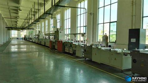
Automated Assembly Line Efficiency Tips
Optimizing PCB assembly workflows requires strategic integration of automation technologies to balance speed and precision. For multi-layer PCB assembly, implementing real-time monitoring systems ensures immediate detection of component misalignment or soldering defects, reducing rework rates. Advanced pick-and-place machines equipped with vision-guided systems enhance accuracy, particularly for high-density interconnects (HDIs), while automated optical inspection (AOI) tools streamline post-placement quality checks.
To maximize throughput, calibrate conveyor systems to synchronize with surface-mount technology (SMT) equipment, minimizing idle time between stages. Modular workstation designs allow flexible reconfiguration for varying PCBA batch sizes, improving adaptability without compromising cycle times. Additionally, predictive maintenance algorithms analyze equipment performance data to preemptively address wear, avoiding unplanned downtime.
Material handling automation, such as robotic feeders for delicate ICs or ultra-thin substrates, reduces human error risks. Pairing these with machine learning-driven process optimization refines solder paste application and reflow profiles, ensuring consistency across layers. By aligning automated workflows with lean manufacturing principles, manufacturers achieve 15-30% efficiency gains while maintaining stringent reliability standards for complex multi-layer PCB assemblies.
Multi-Layer PCB Failure Analysis Solutions
Effective multi-layer PCB assembly requires robust strategies to diagnose and resolve failures that compromise functionality. Common defects like delamination, via cracking, or signal distortion often stem from design flaws, material mismatches, or process inconsistencies during PCBA. A systematic approach begins with electrical testing to isolate short/open circuits, followed by thermal imaging to detect hotspots caused by poor thermal management. Advanced techniques such as cross-sectional analysis help visualize internal layer integrity, revealing issues like incomplete lamination or microvia voids.
To optimize PCB assembly reliability, manufacturers integrate automated optical inspection (AOI) and X-ray inspection systems into quality workflows, ensuring precise identification of solder joint defects or misaligned components. For complex failures, time-domain reflectometry (TDR) aids in tracing impedance mismatches affecting signal integrity. Root cause analysis should correlate findings with design files and production parameters—such as reflow profiles or lamination pressures—to prevent recurrence. By implementing these methodologies, PCBA teams reduce rework costs and enhance product longevity, aligning failure diagnostics with proactive design improvements.
Conclusion
Successful multi-layer PCB assembly requires a holistic approach that integrates design foresight, precision manufacturing, and rigorous validation. By aligning design considerations with material selection and lamination process control, manufacturers can mitigate risks such as delamination or signal distortion. Advanced automation in PCBA lines further enhances consistency, reducing human error and accelerating throughput.
Equally critical is the implementation of quality assurance protocols, including thermal cycling tests and impedance verification, to ensure long-term reliability in demanding environments. Proactive failure analysis not only resolves immediate defects but also informs iterative improvements across the production lifecycle.
Ultimately, optimizing multi-layer PCB assembly hinges on balancing technical expertise with adaptive problem-solving. Whether addressing signal integrity challenges or refining thermal management strategies, each decision must align with the end application’s performance requirements. This interdisciplinary effort transforms complex layer stacking into robust, high-performance electronics ready for real-world deployment.
FAQs
What distinguishes standard PCB fabrication from multi-layer PCBA?
Standard PCB assembly focuses on single/double-layer boards, while multi-layer PCBA involves interconnecting 4+ conductive layers through precision lamination and laser-drilled vias. This complexity demands stricter dielectric material selection and thermal stress management.
How does material choice affect multi-layer PCB reliability?
Using high-Tg FR-4 substrates and low-loss prepregs prevents delamination during PCBA reflow cycles. Inadequate materials can cause signal integrity issues or z-axis expansion failures in high-density designs.
What quality tests ensure robust multi-layer PCB performance?
Automated optical inspection (AOI) verifies solder joint integrity, while time-domain reflectometry checks impedance consistency. Thermal cycling tests simulate 5+ years of operational stress to validate layer bonding durability.
Why is controlled impedance critical in multi-layer designs?
Mismatched trace impedance between layers creates signal reflection and crosstalk, especially in >6GHz applications. PCB assembly teams use 3D field solvers to model stackup configurations before production.
Can existing SMT lines handle multi-layer PCBA requirements?
Yes, but upgrades like nitrogen reflow ovens and X-ray inspection systems are recommended. For boards with >12 layers, step-stencil printing ensures even solder paste distribution on microvia pads.
Optimize Your Multi-Layer PCB Assembly Today
For tailored PCBA solutions integrating these best practices, please click here to consult our engineering team.