Mastering PCB Design and Fabrication Techniques for Success

Key Takeaways
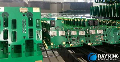
Mastering PCB design and fabrication is crucial for anyone seeking to create high-quality electronic circuits. The primary goal should always be to ensure reliability and performance while keeping production timelines efficient. One of the most significant aspects to remember is the importance of effective PCB assembly or PCBA. Each step in the design process, from initial concept to final assembly, plays a vital role in the overall functionality of the product.
Utilizing advanced software tools can significantly enhance design accuracy while effectively allowing for complex layouts and routing techniques. It’s essential to meticulously plan your circuit pathways, ensuring that component placement minimizes interference and optimizes signal integrity. Furthermore, meticulous attention during the fabrication process can prevent common pitfalls that lead to circuit failures.
Below is a table summarizing key considerations in both design and fabrication processes:
| Aspect | Consideration |
|---|---|
| Initial Design | Define requirements and select components carefully |
| Software Tools | Invest in reliable PCB design software |
| Component Placement | Strategically place components to reduce noise and improve functionality |
| Routing Techniques | Implement proper layer stack-up and tracing techniques |
| Fabrication Quality | Choose a reputable manufacturer for high-quality PCBs |
By honing these essential skills and incorporating best practices, you will elevate your projects, ensuring successful outcomes in your electronics endeavors. Prioritizing precision throughout both the PCB design and fabrication phases will ultimately lead to enhanced performance of your final product.
Introduction to PCB Design and Fabrication
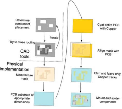
PCB design and fabrication is a critical aspect of electronics that combines creativity with precision engineering. At its core, PCB design refers to the conceptualization of circuit layouts that determine how various electronic components connect and interact within a device. Successful pcb assembly hinges on several fundamental principles, including the understanding of electrical properties, component placement, and signal integrity. The design process often begins with software tools that provide capabilities for schematic capture and layout creation. As you develop your skills in pcba, it is essential to consider factors like heat dissipation, power distribution, and potential electromagnetic interference which can significantly affect circuit performance. Furthermore, effective fabrication techniques must be employed to ensure that the final product meets both safety standards and operational specifications. By mastering these foundational aspects of PCB design and fabrication, individuals can not only enhance their project outcomes but also innovate within the ever-evolving landscape of electronics.
Essential Tools for Effective PCB Design
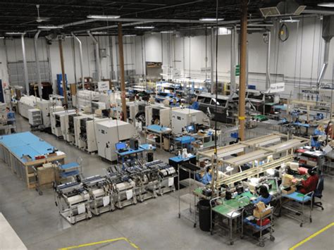
When embarking on the journey of PCB design and fabrication, utilizing the right tools is crucial for achieving successful outcomes. A robust design software suite, such as Altium Designer, Eagle, or KiCAD, provides a comprehensive platform for creating intricate layouts. These tools often come equipped with simulation capabilities that are vital for predicting circuit behavior before the fabrication phase begins. In addition, incorporating PCB assembly tools can streamline the transition from design to real-world application. For those engaged in PCBA, an understanding of soldering techniques and stencil printing options is essential to ensure components are accurately placed and securely affixed. Furthermore, investing in high-quality components and testing equipment can significantly enhance the reliability of your finished project. With these essential tools at hand, designers can minimize errors and optimize their workflows, ultimately leading to high-quality circuits that meet their intended specifications.
Best Practices in PCB Layout and Routing
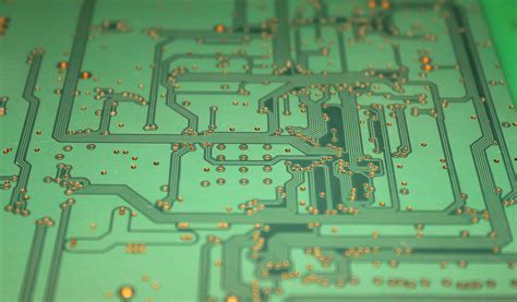
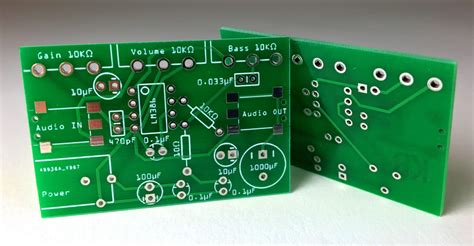
When it comes to PCB design, the layout and routing of components play a significant role in ensuring the effectiveness and reliability of the finished product. Best practices in this area involve careful consideration of various factors that can impact circuit performance and longevity. First, it’s essential to maintain a good signal integrity by minimizing the lengths of traces and avoiding sharp bends; this can reduce electromagnetic interference (EMI) and crosstalk between adjacent traces. Additionally, using ground planes effectively can provide a solid reference point for signal routing, which further enhances electrical performance.
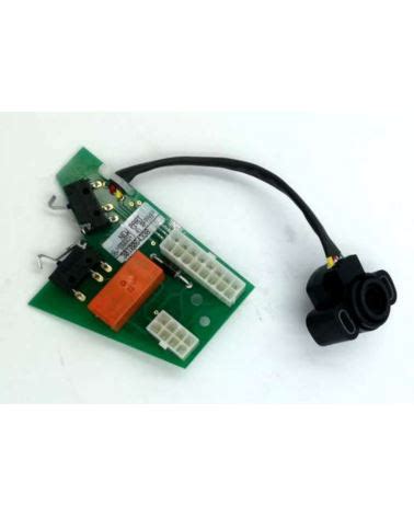
Incorporating proper component placement is another vital aspect; this means positioning components based on their function while keeping heat-sensitive parts away from heat-generating elements. It is crucial to ensure that high-frequency components are located optimally within the layout to enhance performance.
Furthermore, when undertaking PCB assembly (PCBA), it’s recommended to follow a consistent layer stack-up to manage power distribution efficiently. This involves ensuring that power traces are wider than signal traces to reduce resistance while maintaining uniformity in routing paths. Employing these layouts should uphold standards that ease the manufacturing process for assembling your printed circuit board.
Finally, don’t overlook test points; these enable easy access during troubleshooting phases after assembly. By integrating these best practices into your PCB design, you not only pave the way for high-quality fabrication but also significantly boost the overall success of your electronic projects.
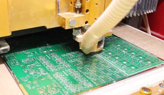
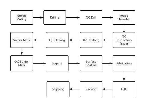
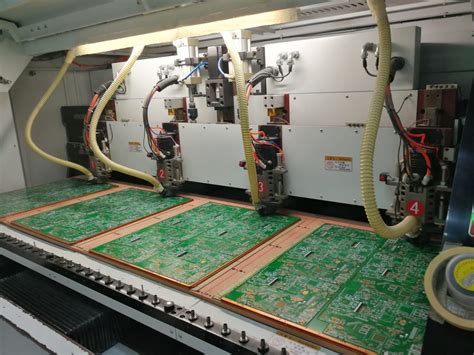
Techniques for High-Quality PCB Fabrication
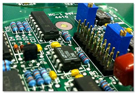
Achieving high-quality PCB fabrication involves several critical techniques that can significantly influence the performance and reliability of your printed circuit boards. First and foremost, the choice of materials plays a vital role in PCB assembly processes. Selecting appropriate substrates, for instance, helps in maintaining the integrity of your circuit designs, ensuring they perform as expected under various conditions. Moreover, implementing precision in the routing of traces can minimize electromagnetic interference (EMI), enhancing signal integrity throughout the PCB.
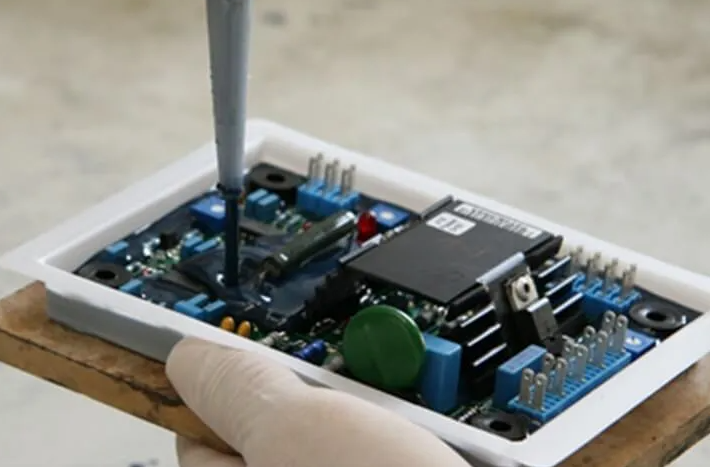
A crucial technique to consider is through-hole or surface mount technology during the PCBA process. Surface mount components often lead to more compact designs while improving yield rates, since they allow for automated processes that reduce human error. Additionally, integrating proper soldering techniques, whether hand soldering or using automated solder machines, is essential in securing reliable connections between components.
“Always use a consistent soldering iron temperature to avoid damaging sensitive components during assembly.” This simple tip can dramatically increase the longevity and performance of your circuits.
After fabrication, thorough testing and inspection should not be overlooked. Utilizing techniques such as X-ray inspection and automated optical inspection (AOI) can help identify discrepancies early on, thus reducing costs associated with debugging later in the project lifecycle. By focusing on these fabrication techniques, engineers and hobbyists alike can ensure successful outcomes in their electronic endeavors while mastering their PCB design skills.
Troubleshooting Common PCB Design Issues
When venturing into PCB design and fabrication, encountering issues during the process is common, but effectively troubleshooting these problems can dramatically improve the quality and functionality of your projects. One of the most prevalent issues is signal integrity, which can lead to cross-talk or interference between traces. To mitigate this, it’s crucial to employ proper layout techniques such as maintaining adequate spacing between high-frequency traces and using ground planes. Another key concern is the reliability of solder joints during PCB assembly (PCBA), which can be compromised by poor thermal management or excessive moisture. Utilizing appropriate soldering methods and ensuring a dry environment are essential steps to ensure robust joints. Additionally, design errors such as incorrect component placement or inadequate pad sizes can result in failed connections during assembly; reviewing your designs with a diligent eye and utilizing software simulation tools can help identify these errors early in the design phase. By implementing these troubleshooting strategies, you not only enhance your circuit’s performance but also streamline the entire production process from PCB design through to successful PCBA, thereby optimizing your electronics endeavors.
Advanced Methods for Enhancing Circuit Performance
When it comes to pcb design and fabrication, leveraging advanced methods can significantly optimize circuit performance. One crucial approach is employing multilayer PCB assembly techniques, which allow for more complex and compact designs without sacrificing functionality. By integrating multiple layers, designers can enhance the routing capabilities, leading to reduced signal interference and improved electrical performance. Additionally, the use of controlled impedance techniques is vital in ensuring that signals maintain their integrity over longer distances within the circuit.
Incorporating high-quality materials in the construction of printed circuit boards (PCBs) also influences performance. Using materials such as FR-4 or even advanced substrates like Rogers can minimize losses and improve thermal management. Furthermore, implementing a robust design for manufacturability (DFM) process early in the design phase is essential to smoothen pcba processes, ensuring that each element integrates seamlessly into the larger system.
Another effective method is the application of simulation tools during the design stage. These tools allow designers to predict circuit behavior under various conditions, optimizing parameters before physical production begins. By analyzing aspects such as signal integrity and thermal performance through software simulations, potential issues can be addressed early on, reducing rework during PCB fabrication.
Lastly, maintaining a focus on component placement and routing strategies significantly impacts circuit performance. Employing techniques such as differential pair routing for high-speed signals ensures that crosstalk is minimized while improving timing accuracy across the board. By prioritizing these advanced methods in your approach to pcb assembly, you can achieve superior circuit functionality and reliability in your electronics projects.
Future Trends in PCB Technology and Design
As we look ahead in the realm of PCB design and fabrication, several key trends are emerging that promise to reshape the industry. One significant advancement is the integration of flexible and organic electronics, which allow for the creation of ultra-lightweight and bendable circuits. These innovations are increasingly demanded in sectors such as wearable technology and IoT (Internet of Things) devices. Moreover, the growth of automated PCB assembly (PCBA) processes aims to enhance production efficiency while minimizing human error. This trend is complemented by advancements in design software, which is becoming more intuitive and powerful, enabling designers to create complex boards with greater ease.
Additionally, sustainability is becoming a pivotal focus, with manufacturers exploring eco-friendly materials and processes to reduce waste during PCB fabrication. This growing awareness not only addresses environmental concerns but also aligns with consumer preferences for sustainable products. The adoption of AI-driven design tools further enhances capabilities in optimizing layouts for improved performance, helping engineers achieve higher signal integrity and reduced electromagnetic interference. As these trends continue to evolve, they will undoubtedly lead to greater efficiencies, improved performance, and groundbreaking applications in electronics that engineers will need to master for ongoing success in their projects.
Conclusion: Elevating Your Electronics Projects Through Mastery of PCB Techniques
Mastering PCB design and fabrication plays a crucial role in enhancing the quality and reliability of your electronics projects. By understanding and applying best practices in PCB layout and routing, you can ensure that your circuit boards are not only functional but also efficient. The importance of quality in the PCB assembly process, often referred to as PCBA, cannot be overstated. A well-executed assembly phase can significantly influence the overall performance of your electronic devices. Utilizing essential tools tailored for effective design allows you to streamline your workflow, making it easier to identify potential challenges early on. As you gain experience, employing advanced methods will enable you to optimize circuit performance and address common design issues proactively. Keeping an eye on future trends in technology will further equip you with insights that can drive innovation in your projects. By mastering these techniques, you contribute not only to successful outcomes but also elevate the standard of quality within the electronics field, ensuring that each project meets or exceeds expectations.
Conclusion: Elevating Your Electronics Projects Through Mastery of PCB Techniques
In the intricate world of PCB design and fabrication, mastering various techniques is crucial for achieving successful project outcomes. By honing your skills in PCB assembly, or PCBA, you can significantly elevate the performance and reliability of your electronic circuits. Focus on the best practices outlined earlier, which emphasize meticulous layout and efficient routing. An understanding of essential tools can greatly enhance your design capabilities, while expert-level knowledge in techniques for high-quality PCB fabrication ensures that your final product meets industry standards. Moving forward, consider incorporating advanced methods for enhancing circuit performance to stay abreast of future trends in PCB technology. Remember, elevating your projects hinges on continuous learning and adapting to evolving practices in this dynamic field, setting you ahead in the rapidly changing landscape of electronics development.
FAQs
What is PCB assembly?
PCB assembly, often referred to as PCBA, is the process of connecting electronic components to a printed circuit board (PCB) to create a functional electronic device. This step is essential for ensuring that the individual components work together effectively.
What are the key steps in PCB assembly?
The key steps in PCB assembly include placing components on the board, soldering the components to secure them in place, and testing the assembled board to ensure functionality. Each step plays a critical role in achieving a high-quality final product.
How does PCB layout affect performance?
The layout of a PCB can significantly impact its performance. Proper routing of traces, minimizing interference, and ensuring adequate spacing between components can enhance signal integrity and reduce noise. Adhering to best practices during layout can lead to more efficient PCBA outcomes.
What tools are essential for PCB fabrication?
Essential tools for PCB fabrication include design software such as CAD programs for creating layouts, soldering stations for connections, and testing equipment like oscilloscopes and multimeters for validation of performance.
What common issues arise during PCB design?
Common issues in PCB design might include signal integrity problems, ground plane issues, and component misplacement. Identifying these problems early through simulation tools can prevent costly errors during pcba.
For improved understanding of your PCB assembly, please click here.
These FAQs provide insights into critical topics related to pcb design and fabrication, helping both beginners and experienced users address common concerns effectively.