Mastering PCB Design for Manufacturing: Optimize Your Production Process
Key Takeaways
In your journey to mastering pcb manufacturing, it’s essential to recognize the significance of effective design for manufacturing in the development of printed circuit boards. By applying best practices early in your design process, you can influence the pcb manufacturing cost significantly, allowing for more competitive pricing from pcb manufacturing companies and improved overall efficiency. Focus on creating layouts that prioritize manufacturability; remember, a well-optimized design minimizes risks and avoids common pitfalls that can arise during production. An understanding of material choices and layer stack considerations will further enhance the performance of your pcb manufacturing business, ensuring a reliable and high-quality end product. Be proactive in communicating with your fabricators, as collaborative efforts can lead to insightful feedback that may refine your designs for maximum yield and performance. Always keep in mind the importance of clearances and feature sizes—these details can make or break your production outcomes, impacting both quality and throughput.
Mastering the Basics of Design for Manufacturing in PCB
When embarking on your journey in PCB manufacturing, it’s crucial to grasp the core principles of design for manufacturing. This foundational knowledge will help you streamline your production process, ultimately leading to high-quality circuit boards and a robust PCB manufacturing business. In your designs, prioritizing manufacturability can significantly reduce PCB manufacturing costs and enhance overall yield.
Start by understanding your chosen PCB manufacturing companies and their specific requirements. Each fabricator may have different capabilities, so aligning your designs with their processes can prevent common pitfalls down the line. Keep in mind essential tips such as optimizing your layout for easier fabrication and ensuring that component placements minimize the need for excessive routing.
“A well-planned PCB design is the first step towards achieving a successful production run.”
Furthermore, do not underestimate the impact of material selection and layer stack considerations on manufacturability. By being proactive about these aspects from the outset, you can markedly improve efficiency and avoid costly revisions during production. Overall, mastering these basics will establish a solid framework for achieving optimal outcomes in your PCB manufacturing efforts.
Key Guidelines for Optimizing PCB Layouts
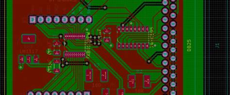
When diving into PCB manufacturing, optimizing your layouts is crucial to achieving a cost-effective and efficient production process. One of the primary considerations is the choice of component placement. Positioning components strategically can significantly enhance the manufacturability of your design. Remember to leave adequate space for assembly tools and ensure that components are easily accessible during the PCB manufacturing process.
You should also pay attention to trace widths and spacing, as these factors impact both electrical performance and the overall PCB manufacturing cost. A well-planned layout can minimize errors during production, which helps in reducing rework and improving yield rates.
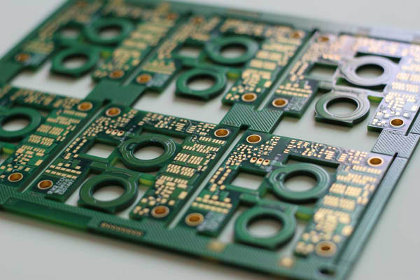
Another vital aspect is to incorporate standard sizes when possible, as this aligns with the specifications commonly used by PCB manufacturing companies. Utilizing standard components not only simplifies sourcing but also keeps costs down.
Here’s a quick reference table for optimized component placement:
| Component Type | Placement Tips | Recommended Spacing |
|---|---|---|
| ICs | Place close to power/ground layers | 0.25 – 0.5 mm |
| Capacitors | Near relevant ICs for effective coupling | 0.5 – 1 mm |
| Resistors | Group with associated circuits | 0.25 – 0.5 mm |
While designing, keep in mind that your layout affects both efficiency in production and reliability post-manufacturing, making it paramount to apply these guidelines rigorously.
By focusing on these strategies, you’ll pave the way for smoother operations with your PCB manufacturing business, ultimately leading to higher-quality products and a more successful outcome in your projects.

Common Pitfalls in PCB Design and How to Avoid Them
When embarking on PCB design, it’s critical to recognize and navigate common pitfalls that could compromise your pcb manufacturing process. One substantial issue arises from overlooking the importance of clearances and feature sizes. Failure to adhere to industry standards can lead to costly mistakes, both in time and pcb manufacturing cost. Additionally, many designers neglect the significance of effective communication with pcb manufacturing companies. Poorly defined design specifications or assumptions about materials can introduce errors that impact manufacturability. To enhance the quality and yield of your circuit boards, ensure that you incorporate thorough checks for all design elements, including proper layer stack considerations. It’s also advisable to consult with your manufacturing partner early in the design phase to identify potential issues local to their processes. This proactive approach not only alleviates risk but can also improve the efficiency of your overall pcb manufacturing business, driving down costs while boosting production reliability. By being mindful of these common pitfalls and implementing strategic measures, you can ensure that your designs yield successful results in both performance and manufacturability.
Understanding Material and Layer Stack Considerations
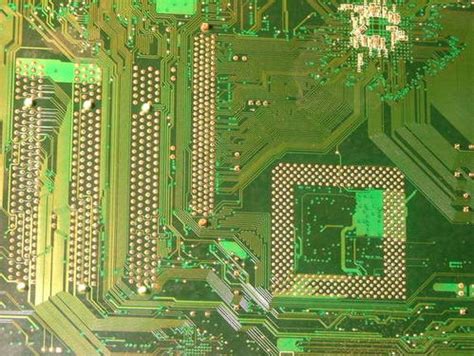
When it comes to pcb manufacturing, understanding your material choices and layer stack configurations is crucial for optimizing the production process. Different materials offer varying levels of conductivity, thermal properties, and dielectric strengths, all of which can significantly impact the pcb manufacturing cost. You should evaluate your project requirements carefully to select materials that not only meet electrical specifications but also align with the capabilities of various pcb manufacturing companies. Layer stack-up is another important aspect—choosing the right configuration affects signal integrity and minimizes issues such as crosstalk or unwanted impedance variations. Each layer in your design serves its purpose, whether it’s providing power distribution, grounding, or signal transmission. By meticulously planning your material and layer stack considerations, you can boost the performance and reliability of your pcb manufacturing business, ultimately enhancing product quality while maximizing yield. Always keep manufacturability in mind during this phase; making informed decisions now will pay dividends in time and cost efficiency later on.
Essential Design Rules for Manufacturability
When diving into PCB manufacturing, understanding the essential design rules can significantly impact both the quality of your product and the efficiency of your production process. You need to prioritize a few key aspects to ensure seamless cooperation with PCB manufacturing companies. First and foremost, keep your design simple by minimizing the number of layers; this can notably reduce the PCB manufacturing cost while enhancing yield rates. It’s crucial to maintain adequate clearances between traces to prevent short circuits and ensure reliable functionality. Moreover, consider using standard component sizes and shapes, as these are typically favored by PCB manufacturing businesses, further simplifying sourcing and reducing production times. Additionally, managing thermal considerations is imperative since heat dissipation can directly affect the longevity and performance of your circuit boards. Lastly, incorporating test points within your designs not only aids in troubleshooting but also aligns with manufacturability best practices, ensuring that you maximize efficiency in PCB manufacturing processes while achieving excellent performance outcomes.
Techniques for Enhancing PCB Yield and Performance
Achieving optimal PCB yield and performance is crucial in the PCB manufacturing process. To start, it’s essential to focus on the design fundamentals that support efficient production. For instance, choosing the right materials can significantly influence both yield and overall costs. You should carefully evaluate material properties to ensure they align with your design requirements while considering factors such as durability and conductivity. Additionally, incorporating design for manufacturability (DFM) principles—like maintaining adequate clearances and avoiding overly complex geometries—can greatly reduce errors during the manufacturing process. It’s also beneficial to engage with experienced PCB manufacturing companies early on to gain insights into their fabrication capabilities, which can help align your design with their processes. By actively addressing potential issues upfront, you can minimize unexpected costs throughout the lifecycle of your PCB manufacturing business, ultimately enhancing your product’s performance while achieving higher yield rates. Focusing on these techniques will not only help in mitigating common setbacks but will also empower you to embark on a more streamlined production journey.
The Importance of Clearances and Feature Sizes in PCB Design
In the realm of PCB manufacturing, understanding the importance of clearances and feature sizes is crucial for ensuring a successful production process. Clearances refer to the spaces between different features on your PCB, such as traces and pads, that allow for proper electrical isolation and prevent short circuits. If these clearances are too small, they can lead to issues during the PCB manufacturing process, potentially causing your board to fail inspection or not perform as intended. On the other hand, overly spacious clearances can lead to increased PCB manufacturing cost, as more material may be used than necessary.
Moreover, feature sizes—like trace width and pad diameter—play a vital role in determining how well your circuit board will function. For instance, traces that are too narrow may not handle the required current load, resulting in overheating or failure. Knowing how to balance these sizes with the capabilities of your chosen PCB manufacturing companies is imperative. Depending on their processes and technologies, different fabricators may have varying tolerances, so it becomes essential for you to communicate effectively with them. This careful consideration not only ensures manufacturability but also enhances quality while maintaining an optimal yield ratio.
By focusing on these elements during the design phase, you pave the way for a successful PCB manufacturing business, minimizing common pitfalls and creating a robust final product that meets both performance standards and budgetary constraints. Remember, effective PCB design isn’t just about aesthetics or functionality; it fundamentally revolves around understanding how these components influence overall performance in real-world applications.
Best Practices for Effective Collaboration with Fabricators
Successful PCB manufacturing hinges on effective collaboration with your fabricators. Establishing a solid relationship is essential for ensuring that your designs translate well into physical products. Start by being transparent about your expectations regarding the PCB manufacturing cost and desired timelines. This openness builds trust and sets the groundwork for a productive partnership. It’s also important to provide detailed design files that adhere to the essential design rules for manufacturability. Doing so reduces miscommunication and minimizes the likelihood of errors during production.
When discussing specifications, pay close attention to how different PCB manufacturing companies approach material selection and layer stack considerations. Each fabricator may have unique capabilities that can influence both performance and cost, which makes it crucial to understand their strengths. Engaging in regular dialogues throughout the design process allows you to make adjustments in real time, ensuring optimal results aligned with your business objectives. Always be prepared to ask for feedback on your designs; this can yield valuable insights into potential improvements and help you tap into the cost-saving opportunities available within different PCB manufacturing processes.
Incorporating feedback from your fabricator not only enhances the quality of your assemblies but also strengthens your continuing relationship, ultimately impacting the success of your PCB manufacturing business. By making collaboration a priority, you improve not just manufacturability but also contribute to higher yields and overall performance of the final circuit boards.
Conclusion
In summary, successful PCB manufacturing hinges on diligent attention to detail throughout the design phase. By mastering the principles of design for manufacturing (DFM), you can significantly influence the overall PCB manufacturing cost and efficiency. It is crucial that you recognize the role of PCB manufacturing companies in this journey, as they often provide invaluable feedback that can help you refine your layouts and specifications. Understanding how to avoid common pitfalls not only enhances the manufacturability of your designs but also ensures higher yields and a more cost-effective production process. When considering your next PCB manufacturing business venture, integrating these guidelines will pave the way for more reliable circuit board outcomes, while also establishing a strong relationship with fabricators. Ultimately, maintaining a focus on these principles is essential for achieving high-quality results in today’s competitive landscape.
FAQs
What is PCB manufacturing?
PCB manufacturing refers to the process of creating printed circuit boards (PCBs) that are essential for electronic devices. This involves several stages, including design, fabrication, and assembly.
How do I choose the right PCB manufacturing companies?
When selecting PCB manufacturing companies, consider their reputation, experience, and the range of services they offer. Reviews and testimonials can provide insight into their past performance and quality standards.
What factors affect PCB manufacturing cost?
The cost of PCB manufacturing can be influenced by factors such as the complexity of your design, the number of layers needed, material selection, and production volume. Understanding these elements can help you estimate your overall expenses more accurately.
How can I enhance the efficiency of my PCB manufacturing business?
To optimize your PCB manufacturing business, focus on improving design for manufacturability principles, maintain clear communication with your team and fabricators, and leverage technology to streamline processes.
What common challenges might I face in PCB production?
Challenges in PCB manufacturing often include miscommunication with manufacturers, misalignment in production specifications, and quality control issues. Being aware of these pitfalls can help you devise effective countermeasures.
For further insights on optimizing your production processes in PCB design, please click here: Master Your PCB Manufacturing.