Mastering the Art of Assembling and Testing Electronic Components on Small PCBs
Key Takeaways
When embarking on the journey of pcb assembly, it is essential to grasp the fundamental concepts that underpin the process. Understanding printed circuit boards (PCBs) is critical, as these intricate components serve as the backbone for connecting electronic elements. A well-crafted pcba (printed circuit board assembly) can enhance the performance and reliability of any electronic project. The importance of utilizing appropriate tools and materials cannot be overstated; precision tools will ensure that components are accurately positioned, while quality materials will lead to superior solder joints. Furthermore, mastering various soldering techniques is a game changer in achieving robust connections without damaging sensitive components. Each step in the assembly process benefits from careful attention to detail—whether it’s proper component placement or employing best practices for inspecting joint quality before proceeding. Don’t overlook troubleshooting; familiarizing yourself with common issues can save valuable time during repairs or iterations. Lastly, implementing effective testing strategies not only verifies the functioning of your pcba, but also elevates your confidence in its reliability, paving the way for successful outcomes in all your electronic projects.
Understanding Printed Circuit Boards: An Introduction
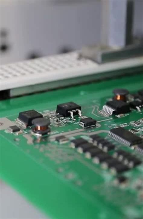
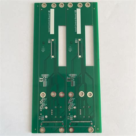
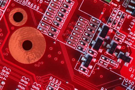
Printed Circuit Boards (PCBs) play a crucial role in modern electronics, serving as the backbone for virtually all electronic devices. Understanding the fundamentals of pcb assembly is essential for anyone looking to work in electronics, whether you are a hobbyist or a professional. At its core, a PCB is designed to house and connect electronic components, allowing them to communicate and function effectively. Each board features conductive pathways etched from copper sheets laminated onto a non-conductive substrate. These pathways facilitate the flow of electricity between components, making it vital to ensure accurate and precise assembly.
In the realm of pcba (Printed Circuit Board Assembly), adherence to best practices ensures reliability and performance. An essential step in this process is selecting the right tools and materials for your assembly needs; high-quality soldering equipment, appropriate solder materials, and effective component handling tools can significantly impact the outcome of your projects. Additionally, understanding how your chosen components interact within the circuit is key to achieving optimal functionality.
“Knowing your components and their specifications can help prevent common mistakes during assembly.”
Whether you are assembling simple circuits or complex designs, a solid grasp of PCB fundamentals will enhance your confidence in tackling any project. The journey from concept to finished PCB involves rigorous testing methods as well; this will be explored further in subsequent sections. Ultimately, mastery over these principles not only leads to successful outputs but also fosters innovation within electronic design projects.
Essential Tools and Materials for PCB Assembly
When embarking on a project that involves PCB assembly (often abbreviated as PCBA), having the right tools and materials is crucial for achieving success. The foundation of a well-executed pcb assembly process lies in a selection of essential items that enhance precision and efficiency. A reliable soldering iron with adjustable temperature settings is among the most important tools; it allows for optimal soldering of electronic components while preventing damage to sensitive parts. Pairing this with high-quality solder wire, preferably with a rosin core, ensures smooth connections that contribute to the longevity and reliability of the finished product.
Additionally, utilizing various hand tools such as tweezers, wire cutters, and needle-nose pliers can significantly aid in the safe handling and placement of components on the circuit board. A sturdy workspace equipped with adequate lighting can also enhance visibility, allowing for meticulous work that is essential during component placement. Furthermore, anti-static wrist straps and mats play an important role in safeguarding electronic components from static discharge, which can adversely affect their functionality.
For those involved in more complex PCB assembly, investing in a hot air rework station can be beneficial. This tool not only facilitates soldering but also allows for easy component replacement when necessary. Lastly, having an assortment of electronic components readily available—such as resistors, capacitors, and integrated circuits—will streamline the assembly process. Collectively, these tools and materials create an optimal environment that fosters successful assembly and testing of small PCBs, ultimately leading to functional electronics that meet project specifications.
Step-by-Step Guide to Soldering Techniques
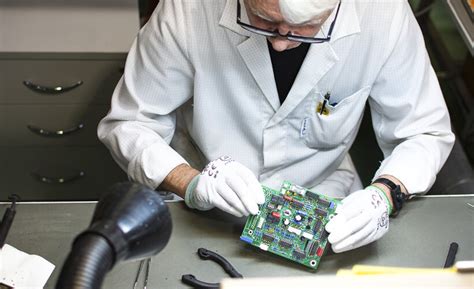
Soldering is a fundamental skill in pcb assembly and is essential for creating reliable connections between electronic components on a small PCB. To begin, ensure that you have the right tools readily available, including a soldering iron, solder wire, and a heat-resistant work surface. Start by properly heating your soldering iron, which should reach a temperature of around 350°C (662°F). This temperature allows for efficient melting of the solder without damaging the components.
Next, you should prepare your PCB by cleaning the pads to ensure there are no contaminants that could interfere with the soldering process. After preparing your workspace and components, it’s time for component placement. Position each electronic element on the PCB according to your design schematic. It’s vital to pay attention to polarity—especially with polarized components like capacitors and diodes—to avoid mistakes.
Once everything is positioned correctly, hold the component in place with tweezers or your fingers while applying heat to the pad and lead simultaneously with your soldering iron. Introduce solder wire into the joint where heat is applied; it should flow smoothly around both components, creating a strong electrical connection. Ensure that you do not add too much solder; excess can lead to bridges or shorts between adjacent pads.
After soldering, allow each joint to cool naturally before moving on to inspection methods. Inspect your solder points visually—look for shiny surfaces which indicate good connections, and check for any cold joints or accidental connections between pads (known as cold solder joints). Following these meticulous steps not only enhances your skills in pcba but also lays down a solid foundation for producing high-quality small PCBs that function reliably in various applications.
Component Placement: Tips for Precision and Efficiency
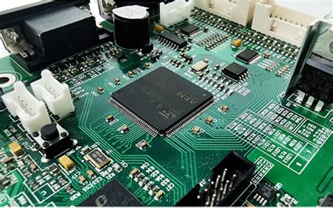
When it comes to pcb assembly, the placement of electronic components on a printed circuit board (PCB) is a critical step that significantly influences the overall performance and reliability of the final product. Achieving precision in component placement not only enhances the aesthetic appeal of your pcba but also minimizes potential issues during soldering and testing phases. To ensure accurate positioning, start by carefully reviewing the schematic diagram and corresponding layout design before you begin. Utilize tools such as tweezers for small components or vacuum pick-ups for ICs to handle delicate pieces with care. It’s also advisable to work in a well-lit area to better visualize the placement points, reducing the chances of misalignment.
Additionally, consider the orientation of polarized components, ensuring they are correctly aligned with designated markings on the PCB. For larger components, a slight tilt can facilitate easier access during soldering, while also optimizing space usage on your PCB. By segmenting your work area into sections dedicated to different types of components, you will streamline your workflow and maintain orderliness in your assembly process. Regularly inspecting component placements before proceeding with soldering can lead to immediate corrections that save time and resources. This forward-thinking approach not only promotes efficiency but also enhances the quality of your pcba, resulting in a product that meets both functional demands and aesthetic standards.
Inspection Methods: Ensuring Quality and Performance
In the realm of pcb assembly, performing meticulous inspections during and after the assembly process is essential for ensuring both quality and performance. Effective inspection methods help to identify defects that may compromise the functionality of a printed circuit board (PCB). Visual inspection is typically the first line of defense, where one examines the solder joints, component alignment, and overall aesthetics. Employing magnification tools can enhance this process, allowing for a more detailed examination of small components often found on small PCBs.
Additionally, automated optical inspection (AOI) systems have become increasingly popular in pcba processes. These systems use cameras and sophisticated software to compare assembled boards against predefined templates, identifying discrepancies with remarkable accuracy. Another vital inspection method is X-ray inspection, particularly useful for boards with components that have leads obscured by others or in blind vias.
After these inspections, implementing electrical testing adds another layer of verification. Techniques such as in-circuit testing (ICT) or functional testing can help to ensure that soldering has been performed properly and that all components are functioning as intended. By utilizing a combination of these inspection methods throughout the pcb assembly process, one can significantly enhance the reliability and durability of small PCBs, ultimately translating to improved performance in their applications.
Troubleshooting Common Issues in Small PCBs
When engaging in pcb assembly, encountering issues is a natural part of the process. Common challenges include poor solder joints, misplaced components, and unintentional short circuits, all of which can severely impact the functionality of your printed circuit board assembly (PCBA). Understanding how to identify and resolve these issues is pivotal for achieving optimal performance.
Common Issues and Solutions Table
| Issue | Description | Solution |
|---|---|---|
| Poor Solder Joints | Weak connections that may lead to intermittent failures | Use proper soldering techniques; ensure adequate heat application |
| Missed Component Placement | Components placed in incorrect positions, leading to circuit failure | Always double-check your schematic and use a reference design |
| Unintentional Short Circuits | Two or more traces connect unintentionally, causing current leaks | Inspect the layout meticulously; use a magnifying tool for small PCBs |
| Component Damage during Soldering | Sensitive components can be damaged by excessive heat | Employ heat sinks and work quickly to minimize heat exposure |
For successful troubleshooting, start with a visual inspection to catch any obvious defects. Implementing systematic testing methods allows for identifying issues that are less visible—like measuring continuity in traces or checking resistance levels across components. Keep in mind that effective troubleshooting is often iterative; addressing one issue may reveal another problem. This continuous refinement is fundamental not only for repairing small PCBs but also for improving overall skills in pcb assembly.
In addition, utilizing tools such as magnifiers or software simulation can provide insights into the underlying problems often overlooked during initial evaluations. Adopting these practices ensures reliability and enhances the success rate of your PCBA, paving the way for proficient project outcomes.
Effective Testing Strategies for Reliable Results
To ensure the success of your pcb assembly processes, implementing effective testing strategies is crucial. Once you have assembled your pcba, the next step involves rigorous testing to identify potential flaws or performance issues. Begin with a thorough visual inspection, checking for solder joint integrity, misplaced components, and any foreign debris that may compromise functionality. Following this, perform electrical tests such as continuity checks and functional tests using a multimeter or an oscilloscope to confirm that each circuit operates as intended. It’s also advisable to employ automated testing equipment when dealing with larger volumes; this can significantly enhance the accuracy and efficiency of your evaluations. Additionally, consider environmental stress testing, which simulates extreme conditions in order to assess the durability and reliability of your assembly in real-world scenarios. By systematically applying these strategies during the testing phase of your pcb assembly, you can dramatically reduce the likelihood of failures and enhance the overall performance of your projects.
Best Practices for Maintaining and Upgrading PCBs
Maintaining and upgrading your PCB assembly is crucial for ensuring longevity and performance. Regular inspections can help identify wear or damage, such as cracked solder joints or corrosion on the pcba connections. When maintaining your printed circuit boards, always start by cleaning the surface to remove dust and grime, which can impact both functionality and aesthetics. For upgrades, consider the benefits of using higher quality components; investing in superior resistors or capacitors may enhance the overall performance of your circuit. If you’re working on a project that requires more power or additional functions, carefully assess whether modifications to your current design can accommodate these changes without compromising reliability. Always document your modifications in detail; this practice will assist in troubleshooting any future issues that may arise. By following these best practices, you will contribute to the performance stability and resilience of your PCBs, paving the way for successful electronic projects ahead.
Conclusion
Mastering pcb assembly is an essential skill for anyone interested in electronics, whether you are a beginner or a seasoned expert. The process of assembling and testing electronic components on small PCBs, or pcba, requires attention to detail and an understanding of various techniques that can significantly impact the functionality of the final product. Through the steps outlined in this article, we have seen that each phase, from soldering to inspection and testing, plays a crucial role in ensuring the reliability of your circuits. Maintaining high standards in component placement is vital—precision can save time during troubleshooting and lead to enhanced performance. Furthermore, implementing effective testing strategies is key to identifying potential issues before they evolve into major problems. The knowledge acquired from this guide will empower you to create small PCBs that not only meet your expectations but also exhibit durability and consistency in performance. As you delve deeper into the world of electronics, remember that mastering these techniques will enhance your skills and expand your possibilities in pcb assembly projects.
FAQs
When diving into the world of pcb assembly, many enthusiasts find themselves with a plethora of questions. One common inquiry is about the differences between PCB and PCBA. While PCB stands for Printed Circuit Board, representing the bare board, PCBA refers to Printed Circuit Board Assembly, indicating a fully assembled circuit board with components soldered onto it. Understanding this distinction is crucial for anyone involved in electronic projects.
Another frequently asked question pertains to the types of solder used in pcb assembly processes. There are various solder types available, including lead-free and lead-based options. Each has its advantages and disadvantages, depending on factors like environmental considerations, melting points, and ease of use. It’s essential to choose the right type based on your specific project requirements.
Many individuals also wonder about the best practices for ensuring proper component placement during assembly. The key is to follow a systematic approach—using tweezers for small components, verifying polarity, and adhering to the designed layout can significantly increase accuracy and efficiency during the PCBA process.
Furthermore, questions regarding troubleshooting common issues abound. For instance, if a circuit isn’t functioning as expected after assembly, checking for cold solder joints or misplaced components is often a good starting point.
Lastly, on testing strategies, many seek guidance on how to effectively test their assembled PCBs to ensure reliability before deployment. Utilizing devices like multimeters or oscilloscopes can help detect faults early in the process.
For anyone looking to further their knowledge or refine their skills in pcb assembly, numerous resources are available online.