Mastering the Art of PCB Assembly: A Step-by-Step Guide for Innovators
Key Takeaways
In the realm of pcb assembly, understanding the foundational elements ensures a successful assembly process. A solid grasp of circuit design, component specifications, and layout principles is crucial for anyone venturing into pcba. Assembly processes can often appear daunting, especially when considering the intricate nature of component placement and soldering. However, with the right approach and understanding of essential tools, one can streamline this journey. The step-by-step assembly process typically includes planning, prototype testing, and iteration to fine-tune designs for optimal performance. Moreover, addressing common challenges such as alignment errors or soldering issues is vital in achieving high-quality results. By incorporating effective strategies for quality control, one can reinforce reliability in their pcb assembly projects. It’s also beneficial to stay updated on current trends and advancements in pcb technology, as this knowledge often sparks innovation and enhances overall design outcomes.
Understanding the Basics of PCB Design
The foundation of successful PCB assembly lies in the design phase, where innovation meets functionality. To ensure an effective Printed Circuit Board (PCB) design, one must grasp the essential elements that define it. The initial step involves creating a schematic diagram that outlines the electrical connections between components. This diagram serves not only as a blueprint but also as a communication tool among team members.
When transitioning from schematic to layout in PCB design, the arrangement of components must prioritize both electronic performance and manufacturability. Factors such as trace width, spacing, and layer stacking need careful attention to prevent issues later in the pcba process. Utilizing simulation tools can help predict potential failure points before physical assembly takes place.
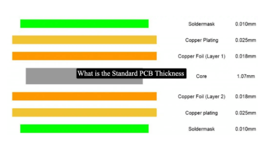
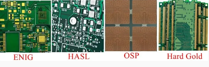
Additionally, selecting appropriate materials is crucial; the choice between different substrates, like FR-4 or Rogers, impacts not only electrical performance but also thermal management during operation. Creating a design for manufacturability (DFM) and testability (DFT) ensures that the finished circuit boards are reliable and efficient.
Here is a summary table outlining key considerations in PCB design:
| Aspect | Importance |
|---|---|
| Schematic Diagram | Blueprint for connections |
| Component Placement | Affects performance and manufacturability |
| Trace Design | Influences electrical characteristics |
| Material Selection | Impacts reliability and heat dissipation |
“Design is not just what it looks like and feels like. Design is how it works.” – Steve Jobs
The early stages of pcb assembly are critical; they lay the groundwork for addressing common challenges that may arise during later phases. By focusing on these foundational elements of design, innovators can enhance their skills in creating high-quality PCBs that meet both functional requirements and industry standards while paving the way for more complex designs in the future.
Essential Tools for PCB Assembly
To successfully navigate the world of PCB assembly (PCBA), having the right tools at your disposal is crucial. The assembly process requires a blend of precision and efficiency, and the tools you choose can significantly influence the outcome. Begin with a quality soldering iron, as it is essential for making reliable connections between components on the circuit board. Pair it with various solder types, such as lead-free or resin-core, to suit your specific requirements. Next, a desoldering pump is indispensable for correcting mistakes, allowing you to remove solder easily without damaging your components.
In addition to these essentials, investing in a good pair of antistatic tweezers will enable you to handle small parts and components with care. An ESD-safe work surface or mat is also recommended to prevent electrostatic discharge that can harm sensitive electronic parts. To ensure accurate placements during assembly, a magnifying lamp can be invaluable for inspecting fine details and ensuring that each connection is secure.
Moreover, consider adding specialized tools such as PCB holders or fixtures that stabilize your board during the soldering process. For those venturing into more advanced techniques, a reflow oven or a hot air rework station can enhance your capability to work with complex assemblies typically found in modern electronics.
Ultimately, selecting the right combination of tools designed for PCB assembly will empower you to achieve superior results whether you’re an amateur enthusiast or an experienced professional. The effectiveness of your assembly process rests heavily on these tools; investing in them wisely not only enhances productivity but ensures top-quality outcomes in every project.
The Step-by-Step Assembly Process
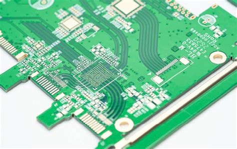
The PCB assembly process is a meticulous journey that requires attention to detail and precision at each stage. To begin, it is crucial to ensure that the printed circuit board assembly (PCBA) layout is thoroughly vetted and meets design specifications. Starting with the placement of components, each element from resistors to integrated circuits needs to be accurately positioned according to the design schematic. This step calls for a careful inspection of the footprints on the board, as even minor misalignments can lead to functionality issues down the line.
Following component placement, the next step is soldering. Utilizing either wave soldering or reflow techniques, it’s important to achieve optimal heat distribution to ensure reliable connections. The choice of solder—whether lead-based or lead-free—can impact not just the performance but also compliance with environmental regulations, which makes it essential for engineers and hobbyists alike to make informed choices about their materials.
Once soldering is complete, transitioning into visual inspection guarantees that all components are properly seated and plated without short circuits or cold joints. Incorporating automated optical inspection (AOI) can yield quicker identification of defects, allowing for real-time adjustments during PCB assembly.
As you progress through the stages, a focus on cleanliness cannot be overstated; residues from soldering can interfere with circuit performance. Regular cleaning protocols should be established prior to final testing. To conclude this phase of PCBA, functional testing will reveal whether all systems are operating correctly according to design specifications. This comprehensive approach not only enhances reliability in your final product but also reinforces good practices for future PCB assembly projects.
Common Challenges and Solutions in PCB Assembly
The process of pcb assembly can present a variety of challenges that may hinder progress or impact the functionality of the final product. One prevalent issue is the alignment of components during assembly. If components are not correctly aligned, this can lead to poor connections or, in some cases, complete failure of the circuit. Utilizing advanced alignment tools and techniques, as well as carefully reviewing designs before assembly, can significantly mitigate these risks.
Another common challenge is soldering defects, such as cold joints or solder bridges. These issues typically arise due to improper temperature control or excess solder. To address this, employing high-quality pcba materials and ensuring precise temperature management during the soldering process is essential. Additionally, implementing automated inspection systems can help detect these defects early on.
Lastly, dealing with component availability can pose significant hurdles in pcb assembly projects. Supply chain disruptions may lead to delays or forced substitutions that jeopardize project timelines and budgets. Maintaining strong relationships with multiple suppliers and staying updated on component trends can help overcome these challenges effectively.
Adopting proactive strategies to manage these common hurdles will not only streamline the pcba process but also enhance overall efficiency and reliability in electronic design projects.
Quality Control: Ensuring Reliability in Your PCB
In the realm of PCB assembly, maintaining high standards of quality is paramount to ensure the reliability of your final product. Quality control processes involve numerous steps and methodologies designed to identify defects and minimize variations in the PCBA process. This begins with thorough inspections during initial production, where visual assessments and automated optical inspections (AOI) can detect solder paste application issues, misaligned components, or any potential short circuits. Moreover, implementing stringent testing protocols such as functional tests, boundary scan tests, and environmental stress tests greatly enhances the reliability of your PCB. It is essential to make use of statistical process control (SPC) tools to monitor production variables over time, which helps in identifying trends that could lead to defects. Documenting each quality control stage within the assembly process not only provides a roadmap for continuous improvement but also builds confidence in your craftsmanship among clients and stakeholders. Ultimately, prioritizing quality control from the outset can save time and resources while ensuring that your PCB assembly yields a product that meets or exceeds industry performance standards.
Tips and Tricks for Efficient Assembly
To enhance your pcb assembly experience, adopting effective strategies can significantly improve the overall process. First and foremost, ensure that your workspace is organized and free of clutter, as this minimizes distractions and allows for greater focus on the intricate details of pcba. Furthermore, familiarizing yourself with the various tools essential for assembly, such as soldering irons, tweezers, and magnifying glasses, is crucial. Each tool has its specific purpose, which can streamline your workflow and boost accuracy in assembly tasks. Additionally, implementing a systematized approach to component placement—following a logical order—is highly beneficial; categorizing parts by their functions or positions can reduce errors and save time. Embracing the use of jigs or fixtures can also enhance efficiency by providing stability and consistency during the soldering process. Finally, remember to take breaks when needed; this will help maintain your focus and energy levels throughout longer assembly sessions. By integrating these tips into your routine, you’ll find that not only does your skill set improve but so does the quality and reliability of your finished pcba projects.
Advanced Techniques for PCB Assembly
As you delve deeper into PCB assembly or PCBA, you may discover several advanced techniques that can significantly enhance your efficiency and the quality of your finished product. One notable method is the implementation of Surface Mount Technology (SMT), which allows for smaller components to be placed directly onto the surface of a circuit board, reducing the overall footprint and improving performance. Utilizing automated assembly processes can also provide precision and speed that manual methods may lack. The introduction of pick-and-place machines allows for accurate placement of components, while wave soldering or reflow ovens ensure reliable connections with minimal defects. Furthermore, adopting design for manufacturability (DFM) principles during your design phase can preemptively address issues that might arise during pcba, ensuring a smoother assembly process. Lastly, integrating rigorous testing methods such as in-circuit testing (ICT) or functional testing can guarantee that each board meets quality standards before moving into production. Embracing these advanced techniques will not only streamline your PCB assembly processes but also pave the way for more innovative designs and cutting-edge applications in electronic development.
Future Trends in PCB Technology
As the world of electronics continues to evolve, the pcb assembly landscape is also undergoing significant transformations. One emerging trend is the increasing integration of flexible PCBs (printed circuit boards), which allow for more compact and lightweight designs. This flexibility enables devices to fit into smaller spaces, catering to the growing demand for portable electronics. Furthermore, advancements in automated assembly techniques are streamlining the PCBA (printed circuit board assembly) process, reducing labor costs and increasing efficiency. The adoption of advanced materials such as high-density interconnect (HDI) technology is leading to faster signal transmission and improved performance for complex electronic devices. Additionally, sustainability is becoming a focal point, with manufacturers seeking eco-friendly materials and processes that minimize waste and energy consumption. As we look to the future, it’s clear that staying ahead of these trends will be crucial for engineers and innovators preparing to tackle the next generation of electronic challenges effectively.
Conclusion
As we wrap up our exploration of pcb assembly, it’s clear that mastering the intricacies of this process is essential for anyone engaged in electronic design and innovation. The journey from initial design considerations to the final quality checks involves numerous steps that demand attention to detail and a solid understanding of the tools and techniques involved in pcba. By incorporating the various tips, tricks, and best practices discussed throughout this guide, you can significantly enhance your assembly skills. Remember that overcoming challenges such as component placement accuracy or soldering issues is part of the learning curve in pcb assembly. Keeping abreast of emerging trends will not only strengthen your foundation but also position you advantageously within the evolving landscape of PCB technology. This resource aims to equip you with the knowledge and confidence needed to excel in your projects, whether you’re a budding engineer or a seasoned expert looking to refine your craft.
FAQs
When delving into the world of PCB assembly, it’s common for both newcomers and seasoned professionals to have questions. A fundamental query often revolves around the differences between PCBA and the components involved. To clarify, PCBA refers to a fully assembled printed circuit board that is ready for integration into electronic devices, while PCB assembly is the actual process of assembling various components onto a circuit board.
Another frequent question pertains to the tools required for an efficient PCB assembly process. Essential tools include soldering irons, pick-and-place machines, and reflow ovens, which are critical for achieving quality and precision during the assembly. Moreover, aspiring engineers often want to understand how to troubleshoot common issues that may arise during pcba processes; this is where familiarity with error detection and repair techniques comes into play.
Finally, many individuals inquire about quality control measures in PCB assembly. Maintaining reliability involves multiple steps, including testing methods such as Automated Optical Inspection (AOI) and functional testing post-assembly to ensure performance standards are met.
For further enlightenment on these topics and more about mastering your skills in pcb assembly, consider enhancing your knowledge through ongoing research and practice.