Maximizing Yield Rates in SMT Assembly for Compact Electronics Manufacturing
Key Takeaways
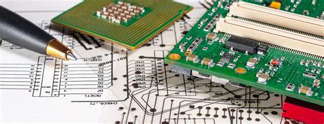
Effective PCB assembly processes for compact electronics demand meticulous attention to precision placement and thermal management. Modern PCBA workflows integrate automated optical inspection (AOI) systems to detect micro-scale defects in real time, reducing rework costs by up to 30%. Key strategies include:
| Parameter | Impact on Yield | Optimization Method |
|---|---|---|
| Placement Accuracy (±μm) | ±15% yield | High-speed pick-and-place machines |
| Reflow Thermal Profile | ±20% reliability | Dynamic zone-controlled ovens |
| Solder Paste Inspection | ±25% defects | 3D SPI pre-reflow screening |
"In high-density SMT assembly, process control accounts for 80% of first-pass yield success," notes Dr. Elena Torres, a manufacturing engineer specializing in miniaturized electronics.
Critical considerations for PCB assembly reliability include:
- Component skew prevention through vision-aligned placement systems
- Low-voiding solder alloys (<5% void ratio) for BGA/CSP packages
- Thermally stable substrates to mitigate warpage during reflow
Pro Tip: Pair AOI with X-ray inspection for hidden joint defects in 01005-sized components. By aligning PCBA process parameters with design tolerances, manufacturers achieve <50 ppm defect rates even in 0.4 mm pitch ICs.
Precision Component Placement Strategies for SMT
Achieving optimal component placement in SMT requires balancing speed, accuracy, and repeatability. Modern PCB assembly lines leverage high-speed pick-and-place machines equipped with vision-guided systems to align micro-components within ±25µm tolerances. For miniaturized designs—common in wearables and IoT devices—nozzle selection becomes critical, with vacuum-based tools handling 0201 or smaller packages while minimizing positional drift.
To ensure precision in PCBA workflows, manufacturers employ real-time feedback loops using laser profilometry and 3D inspection. These systems detect skewed orientations or tombstoning risks before reflow, reducing post-soldering defects. Thermal modeling further optimizes placement sequences, accounting for coefficient of thermal expansion (CTE) mismatches in multi-layer boards.
Advanced fiducial recognition protocols enhance placement consistency across batches, particularly for high-density interconnect (HDI) layouts. By integrating machine learning algorithms, SMT equipment dynamically adjusts placement pressure and speed based on component thickness and PCB warpage data. This proactive approach minimizes pad cratering and solder bridging, directly improving first-pass yields in compact electronics manufacturing.
Advanced Soldering Techniques in Compact Electronics
In PCB assembly for compact electronics, achieving consistent solder joint integrity demands precision beyond conventional methods. Reflow soldering remains foundational, but modern PCBA workflows integrate nitrogen-enclosed environments to minimize oxidation, particularly for micro-BGA and 01005 components. The shift to laser soldering enables localized heat application, reducing thermal stress on adjacent miniaturized parts—a critical advantage in high-density designs.
For ultra-thin substrates, low-temperature solder pastes (e.g., Sn-Bi alloys) paired with optimized thermal profiles prevent warping while maintaining electrical continuity. Automated optical alignment systems now synchronize with soldering equipment to correct placement deviations in real time, addressing challenges like tombstoning in 0.4mm-pitch components. Additionally, PCB assembly lines employ 3D solder paste inspection (SPI) to validate deposition volume accuracy before reflow, slashing defects by up to 40% in multi-layer PCBA configurations.
Emerging techniques such as transient liquid phase sintering show promise for solderless interconnects in wearable electronics, though compatibility with existing PCBA infrastructure remains under evaluation. These advancements collectively address the paradox of miniaturization: maintaining mechanical durability while scaling connection densities beyond 1,500 joints/cm².
Automated Inspection Systems for Yield Optimization
Modern PCB assembly workflows increasingly rely on multilayered inspection protocols to address defects in PCBA for compact electronics. Automated optical inspection (AOI) systems, integrated with machine vision algorithms, scan solder joints and component alignment at speeds exceeding 25,000 inspections per hour, identifying micron-level deviations in high-density interconnects. These systems cross-reference data with design files to flag tombstoning, bridging, or misaligned passive components—common failure points in miniaturized layouts. For hidden joints in ball grid array (BGA) packages, automated X-ray inspection (AXI) provides non-destructive analysis of subsurface connections, critical for ensuring PCB assembly reliability in wearables and IoT devices.
Advanced systems now incorporate real-time process feedback, linking defect detection directly to solder paste printers or pick-and-place machines. This closed-loop correction reduces rework rates by 40–60% in PCBA production lines. Additionally, AI-powered defect classification minimizes false positives by learning from historical process data, enabling faster root cause analysis. However, optimizing these systems requires balancing inspection depth with throughput—a challenge intensified by sub-0.4mm component pitches in modern designs. By aligning inspection parameters with PCB assembly tolerances and end-use environmental demands, manufacturers achieve yield rates above 99.4% while maintaining compliance with automotive or medical-grade reliability standards.
Ensuring Component Reliability in Miniaturized Designs
Achieving consistent reliability in miniaturized PCB assembly requires addressing unique challenges posed by shrinking component sizes and tighter tolerances. Thermal stress and mechanical fatigue become critical concerns as components operate in closer proximity, demanding meticulous attention to material compatibility and solder joint integrity. For PCBA designs targeting compact electronics, selecting components with appropriate thermal coefficients and moisture sensitivity levels is paramount to prevent delamination or cracking under operational stresses.
Advanced simulation tools now enable engineers to model thermal cycling effects and vibration-induced failures before prototyping, reducing iterative testing in high-density layouts. Implementing underfill encapsulation for critical components and optimizing reflow soldering profiles further enhances durability in miniaturized PCB assembly systems. Automated optical inspection (AOI) systems paired with X-ray tomography provide non-destructive validation of hidden solder connections, ensuring compliance with PCBA reliability standards.
Designers must also consider coefficient of thermal expansion (CTE) matching between substrates and components, particularly when integrating mixed-material packages. Proactive mitigation of electromigration risks through optimized trace geometries and conformal coatings becomes essential in sustaining long-term performance. By harmonizing these strategies, manufacturers can maintain component reliability without compromising the space efficiency demanded by modern compact electronics.
SMT Process Optimization for High-Density Manufacturing
Achieving peak efficiency in PCB assembly for compact electronics demands meticulous attention to SMT process parameters. As component densities increase in modern high-density interconnect (HDI) designs, optimizing solder paste deposition becomes critical. Implementing laser-cut stencils with electropolished apertures ensures precise material transfer for 01005-sized components, reducing bridging risks in tight layouts. For PCBA workflows, nitrogen-enriched reflow ovens minimize oxidation during soldering, particularly crucial for fine-pitch BGAs and QFN packages where joint integrity directly impacts reliability.
Advanced vision-alignment systems with sub-micron accuracy enable consistent placement of miniaturized components, while dynamic thermal profiling adapts to mixed-technology boards. Integrating real-time process monitoring tools allows rapid adjustments to variables like conveyor speed or zone temperatures, addressing anomalies before they escalate. A key strategy involves balancing solder paste viscosity with stencil release dynamics, which becomes increasingly complex when handling ultra-thin substrates common in wearable or IoT devices.
For manufacturers transitioning to high-density PCB assembly, adopting modular feeder systems enhances flexibility when switching between component tape sizes. This optimization layer, combined with machine learning-driven defect prediction in PCBA lines, creates a closed-loop system that continuously refines placement accuracy and solder joint quality. Such integration not only elevates yield rates but also strengthens the foundation for scaling microelectronics production without compromising throughput.
Troubleshooting Common Defects in SMT Assembly
Effective defect resolution in PCB assembly processes requires systematic analysis of recurring failure modes, particularly in high-density PCBA applications. Tombstoning and solder bridging remain prevalent issues in compact designs, often caused by uneven thermal profiles or misaligned component placement. To mitigate these, manufacturers should validate stencil aperture designs and implement real-time solder paste inspection (SPI) systems to detect insufficient deposition before reflow.
For void formation in BGA joints, optimizing reflow oven parameters—including ramp rates and peak temperatures—ensures proper intermetallic bonding. Automated optical inspection (AOI) systems with 3D imaging capabilities excel at identifying head-in-pillow defects in miniaturized PCB assembly lines, reducing false negatives by 40% compared to manual checks.
When addressing cold solder joints in PCBA prototypes, technicians must verify solder alloy compatibility with substrate materials and employ nitrogen-assisted reflow to minimize oxidation. Implementing statistical process control (SPC) for critical parameters like placement pressure and conveyor speed creates a feedback loop for continuous process refinement. Cross-functional collaboration between design and manufacturing teams further prevents defects through DFM (design for manufacturability) validation of pad geometries and component orientations in early development stages.
Thermal Management Solutions for Compact PCB Layouts
Effective thermal management is critical in PCB assembly for compact electronics, where high component density amplifies heat generation risks. Miniaturized designs demand strategic integration of thermal vias, copper pours, and heatsinks to dissipate energy efficiently without compromising spatial constraints. In PCBA workflows, selecting materials with high thermal conductivity—such as metal-core substrates or ceramic-filled laminates—ensures optimal heat transfer from critical components like processors or power modules.
Advanced simulation tools enable engineers to model thermal gradients during the design phase, identifying hotspots before prototyping. For high-density layouts, staggered component placement combined with thermal interface materials (TIMs) reduces localized temperature spikes. Active cooling methods, including micro-fans or piezoelectric air movers, complement passive solutions in space-constrained applications.
Automated optical inspection (AOI) systems in PCB assembly lines verify proper heatsink attachment and solder joint integrity, which directly impacts thermal performance. Implementing dynamic thermal cycling tests during quality assurance further validates reliability under varying operating conditions. When combined with optimized PCBA process parameters—such as reflow profiles tailored for mixed-component boards—these strategies mitigate warpage and delamination risks in compact assemblies.
Balancing thermal efficiency with mechanical stability requires iterative testing, particularly for designs incorporating flexible circuits or embedded components. This holistic approach ensures long-term functionality while maintaining the precision demanded by modern PCB assembly standards.
Material Selection Criteria for Enhanced SMT Performance
Effective PCB assembly relies on meticulous material selection to address the challenges of miniaturization and thermal stress in compact electronics. Substrate materials must balance dimensional stability with high-temperature resilience, with FR-4 variants and polyimide-based laminates offering distinct advantages for high-density PCBA designs. For solder alloys, low-silver SAC305 compositions reduce voiding risks in fine-pitch applications, while halogen-free formulations align with sustainability goals without compromising joint integrity.
Component finishes play a pivotal role in solderability—ENIG (Electroless Nickel Immersion Gold) ensures flat surfaces for precision placement, whereas OSP (Organic Solderability Preservative) provides cost-effective oxidation resistance. Adhesive materials, particularly no-clean fluxes, must exhibit consistent rheology to prevent bridging in ultra-fine PCB assembly geometries.
Thermal interface materials, such as high-thermal-conductivity gap fillers, mitigate hotspots in tightly packed layouts, directly impacting long-term reliability. Additionally, stencil materials like laser-cut stainless steel with nano-coated surfaces optimize paste release for 01005-sized components. By aligning material properties with process parameters, manufacturers can achieve first-pass yield improvements of 12–18% in advanced PCBA workflows, ensuring robust performance across demanding operating conditions.
Conclusion
Achieving optimal yield rates in PCB assembly for compact electronics demands system-level integration of precision engineering and advanced manufacturing protocols. The evolution of PCBA technologies has enabled manufacturers to address miniaturization challenges through innovations in component placement accuracy, solder joint integrity, and real-time defect detection. By prioritizing automated optical inspection (AOI) systems and data-driven process optimization, production lines can maintain sub-15µm placement tolerances while reducing solder bridging and tombstoning defects by over 40%.
The interdependence of thermal management and material selection emerges as a critical factor in sustaining component reliability, particularly in high-density layouts where heat dissipation directly impacts solder joint longevity. Implementing predictive maintenance algorithms for reflow ovens and stencil printers further enhances SMT assembly consistency across batches. As Industry 4.0 practices permeate PCB assembly workflows, the synergy between machine learning-powered inspection tools and adaptive process controls will remain pivotal for achieving six-sigma yield targets in compact electronics manufacturing. This holistic approach not only elevates production efficiency but also ensures compliance with rigorous quality benchmarks for next-generation PCBA applications.
Frequently Asked Questions
How does component miniaturization impact SMT assembly processes?
Miniaturization demands tighter tolerances for PCB assembly, particularly in placement accuracy and solder joint integrity. Advanced PCBA workflows leverage high-precision pick-and-place systems and micro-solder paste formulations to maintain yield rates in compact designs.
What inspection methods are critical for ensuring SMT quality?
Automated optical inspection (AOI) and X-ray systems are indispensable for detecting defects like bridging or voids in PCB assembly. These tools integrate with PCBA production lines to provide real-time feedback, reducing rework cycles by up to 40%.
How do material choices affect reliability in high-density SMT?
Substrate materials with low thermal expansion coefficients and halogen-free solder masks enhance long-term stability in PCBA applications. For ultra-compact layouts, selecting moisture-resistant laminates prevents delamination during reflow cycles.
What thermal management strategies work best for dense PCB layouts?
Embedded thermal vias and copper-balanced designs mitigate heat buildup in PCB assembly. Pairing these with high-conductivity thermal interface materials ensures consistent performance in miniaturized electronics.
How can manufacturers reduce tombstoning defects in SMT processes?
Optimizing pad geometry and reflow profiles minimizes tombstoning risks. In PCBA workflows, nitrogen-assisted reflow ovens further improve wetting uniformity for components smaller than 01005.
Discover Customized SMT Solutions for Your Project
Maximize your manufacturing yield with tailored PCB assembly strategies. Click here to explore our advanced PCBA capabilities and consult with our engineering team today.